
Organic semiconductor material containing amine oxide group and application thereof in OLED (organic light-emitting diode) device

An organic semiconductor and amine oxide technology, which is applied in semiconductor devices, semiconductor/solid-state device manufacturing, electric solid-state devices, etc., can solve the problem of poor hole injection/transport performance of PVK, low conductivity, reduced OLED device life and Stability and other issues, to achieve the effect of large-scale industrialization, high conductivity, and avoid adverse effects

Active Publication Date: 2014-08-06
HAIMEN BIWEI INTPROP SERVICE CO LTD
View PDF2 Cites 0 Cited by
  • Summary
  • Abstract
  • Description
  • Claims
  • Application Information

AI Technical Summary

Problems solved by technology

Among them, PEDOT:PSS is the most commonly used, but PEDOT:PSS is actually an acidic solution, which has a certain corrosion effect on the ITO anode, so using PEDOT:PSS as the hole injection layer will reduce the life and stability of OLED devices.
Since PVK is a non-conjugated polymer with a main chain, its electrical conductivity is not high, so the hole injection / transport performance of PVK is not very good, which is also one of the unfavorable factors affecting the performance of OLED devices.

Method used


Image

  • Organic semiconductor material containing amine oxide group and application thereof in OLED (organic light-emitting diode) device
  • Organic semiconductor material containing amine oxide group and application thereof in OLED (organic light-emitting diode) device
  • Organic semiconductor material containing amine oxide group and application thereof in OLED (organic light-emitting diode) device

Examples


Embodiment 1

[0026] Preparation of 4,4-dibromo-2-nitrobiphenyl (1)

[0027] Dissolve 4,4-dibromobiphenyl (20g, 64mmol) in glacial acetic acid (300mL), heat and stir at 110°C, add concentrated nitric acid (70%, 132mL) dropwise to glacial acetic acid, heat for 6h until solid Slowly dissolve, then cool to room temperature. The reaction solution was filtered, the solid was washed with water, and then recrystallized with ethanol to obtain a yellow solid (17.6g, yield77%). 1 H-NMR (300MHz, CDCl 3 ): (ppm) 8.32 (d, 2H), 8.29 (d, 2H), 7.77 (dd, 2H).

Embodiment 2

[0029] Preparation of 2,7-dibromocarbazole (2)

[0030] Triethyl phosphate (60 mL) added with compound 1 (16.5 g, 46.1 mmol) was heated to reflux for 18 h under nitrogen protection. The excess solvent was distilled off from the reaction liquid under reduced pressure, and the residue was dissolved with a small amount of dichloromethane, then precipitated with petroleum ether to obtain the initial product, and then a white solid (9.28 g, yield 62%) was obtained by silica gel / petroleum ether column chromatography. 1 H-NMR (300MHz, CDCl 3 ): δ (ppm) 8.20 (br, 1H, NH); 7.92 (d, 2H); 7.56 (d, 2H); 7.35 (dd, 2H).

Embodiment 3

[0032] Preparation of p-methylphenyl-1-bromo-6-hexyl ether (3)

[0033] Add p-cresol (28g), 1,6-dibromohexane (220mL), potassium carbonate (60g), tetrabutylammonium bromide (3.8g) and acetone (150mL) into a 500mL flask, heat and stir to reflux 48h. The reaction was cooled to room temperature, filtered, and the filtrate was spun with a circulating water pump until the mass was no longer reduced, then distilled under reduced pressure with an oil pump, and the fraction collected at 210°C to 220°C was a colorless oily product (53.5g, yield76.1%). 1 H-NMR (300MHz, CDCl 3 ): δ (ppm) 7.10 (d, 2H); 6.82 (d, 2H); 3.96 (t, 2H); 3.45 (t, 2H); 2.32 (s, 3H); 1.8 (br, 8H).


PUM

PropertyMeasurementUnit
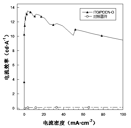
current efficiencyaaaaaaaaaa

Abstract

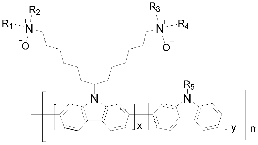
The invention discloses an organic semiconductor material containing amine oxide groups and its application in OLED devices. The polymer main chain of the organic semiconductor material containing amine oxide groups in the present invention is conjugated, and the polymer main chain is composed of carbazole groups with good hole injection / transport properties, and has high electrical conductivity. It is beneficial to the injection and transport of holes in OLED devices.

Description

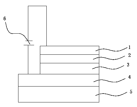
technical field [0001] The invention relates to the field of organic semiconductor optoelectronic materials, in particular to an organic semiconductor material containing an amine oxide group and its application in a hole injection layer of an OLED device. Background technique [0002] like figure 1 As shown, the OLED device is mainly composed of a cathode 1 , a light emitting layer 2 , a hole injection layer (HIL) 3 , an anode 4 , and a substrate 5 sequentially stacked, and a power source 6 is connected to the cathode 1 and the anode 4 . The light-emitting layer 2 is an organic material. When preparing an OLED device, usually on the substrate 5, indium tin oxide (ITO) is first set as the anode 4, then the hole injection layer (HIL) 3 is set on the ITO anode 4, and then the light emitting layer is set on the hole injection layer 3. layer 2, and finally a metal cathode 1 is vapor-deposited on the light-emitting layer 2, for example, a layer of CsF and a layer of metal Al ar...

Claims


Application Information

Patent Timeline
Patent Type & Authority Patents(China)
IPC IPC(8): C08G61/12C07D209/86H01L51/54
Inventor 不公告发明人
Owner HAIMEN BIWEI INTPROP SERVICE CO LTD
Learn More