Wave crest soldering technique of printed circuit board
A printed circuit board and wave soldering technology, which is applied to the assembly of printed circuits with electrical components, can solve problems such as destructive effects, device performance effects, secondary heating of through-hole devices, etc., to improve efficiency, be easy to implement, and prevent The effect of the secondary heating problem
- Summary
- Abstract
- Description
- Claims
- Application Information
AI Technical Summary
Problems solved by technology
Method used
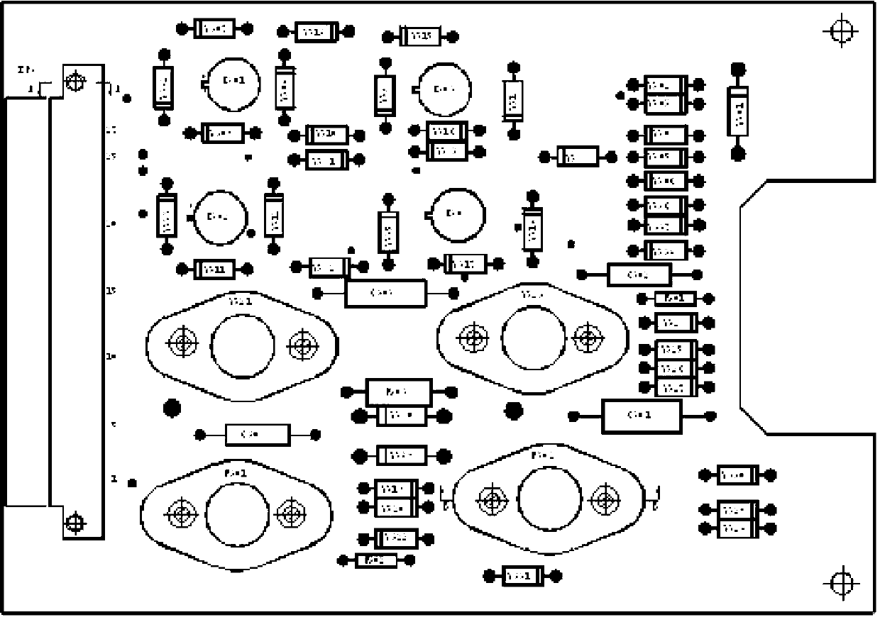
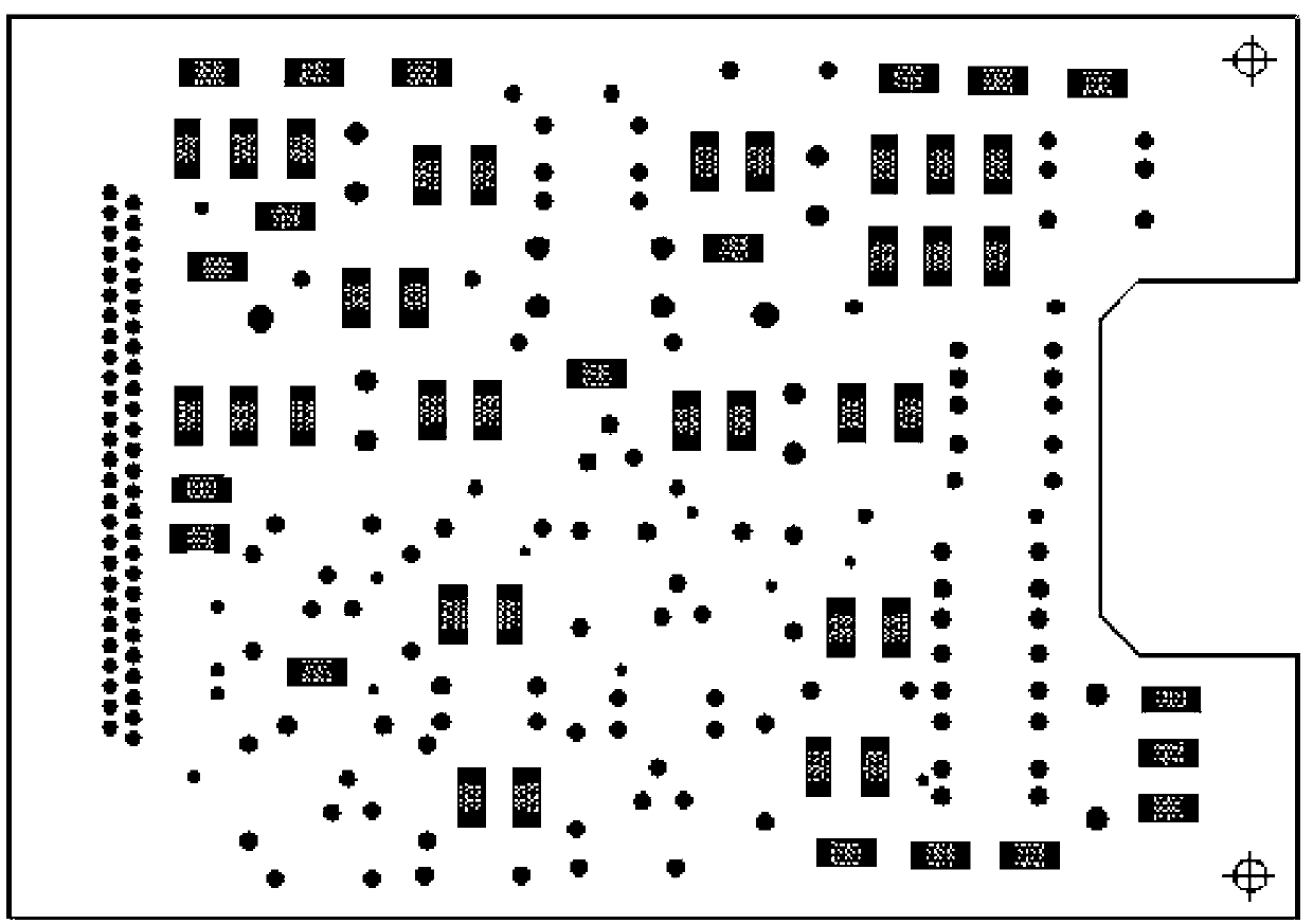
Image

Examples
Embodiment 1
[0019] Example 1: The size code of the components is 0402
[0020] Step 1: Dot red glue in the middle of the pad of the SMT device on the welding surface, and the amount of glue dispensed is 0.0005ml;
[0021] Step 2: Then stick the patch device on the pad, put it in an oven, and bake it at 85±10°C for 30 minutes to cure the red glue;
[0022] Step 3: Take it out and let it cool down to room temperature, then bend, insert, spot-fix and cut the pins of the through-hole device;
[0023] Step 4: Use wave soldering and then print the board, so that the SMT devices are soldered together.
Embodiment 2
[0024] Example 2: The size code of the components is 0603
[0025] Step 1: Dot red glue in the middle of the pad of the SMD device on the welding surface, and the amount of glue dispensed is 0.001ml;
[0026] Step 2: Then stick the patch device on the pad, put it in an oven, and bake it at 85±10°C for 30 minutes to cure the red glue;
[0027] Step 3: Take it out and let it cool down to room temperature, then bend, insert, spot-fix and cut the pins of the through-hole device;
[0028] Step 4: Use wave soldering and then print the board, so that the SMT devices are soldered together.
Embodiment 3
[0029] Example 3: The size code of the components is 0805
[0030] Step 1: Dot red glue in the middle of the pad of the SMD device on the welding surface, and the amount of glue dispensed is 0.002ml;
[0031] Step 2: Then stick the patch device on the pad, put it in an oven, and bake it at 85±10°C for 30 minutes to cure the red glue;
[0032] Step 3: Take it out and let it cool down to room temperature, then bend, insert, spot-fix and cut the pins of the through-hole device;
[0033] Step 4: Use wave soldering and then print the board, so that the SMT devices are soldered together.
PUM
 Abstract
Description
Claims
Application Information
 - R&D
- Intellectual Property
- Life Sciences
- Materials
- Tech Scout
- Unparalleled Data Quality
- Higher Quality Content
- 60% Fewer Hallucinations
Browse by: Latest US Patents, China's latest patents, Technical Efficacy Thesaurus, Application Domain, Technology Topic, Popular Technical Reports.
© 2025 PatSnap. All rights reserved.Legal|Privacy policy|Modern Slavery Act Transparency Statement|Sitemap|About US| Contact US: help@patsnap.com