A method for optical excitation to generate spin-polarized electrons and spin currents
A technology of spin-polarized electrons and spin currents, which is applied in circuits, electrical components, semiconductor devices, etc., can solve the problems of low temperature and low spin polarizability, and facilitate close integration, integration and miniaturization The effect of modernization and strong compatibility
- Summary
- Abstract
- Description
- Claims
- Application Information
AI Technical Summary
Problems solved by technology
Method used
Image
Examples
Embodiment 1
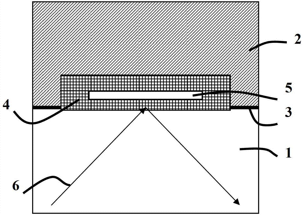
[0031] figure 1 It is a schematic diagram of the principle of Embodiment 1 of the present invention, such as figure 1 As shown, the glass 1 and the air 2 form a total reflection interface 3, and there is a functional layer 4 that generates spin-polarized electrons and spin currents on the interface 3, and the functional layer 4 contains a structure composed of a surface plasmon metal material 5. The light wave 6 is totally reflected from the glass 1 to the interface 3 at an incident angle greater than the critical angle of total reflection. The interaction of the formed structures 5 generates spin-polarized electrons and spin currents in the functional layer 4 .
[0032] The structure 5 made of surface plasmon metal material in the functional layer 4 can be but not limited to the following structures:
[0033] (1) A 30nm thick Au film prepared on the glass surface by electron beam evaporation technology.
[0034] (2) A 200nm thick Al film prepared on the glass surface by v...
Embodiment 2
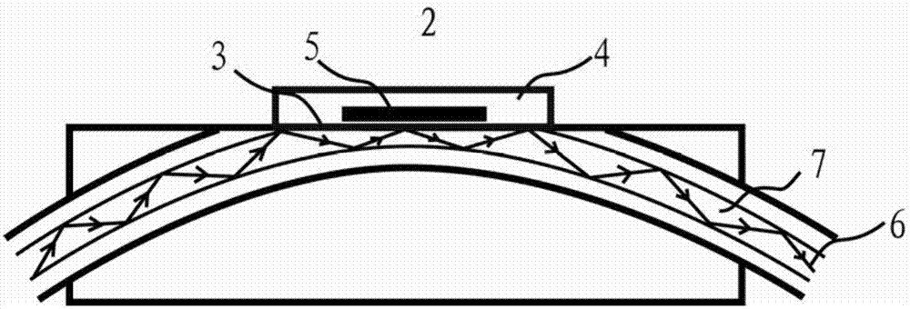
[0042] figure 2 It is a schematic diagram of the principle of Embodiment 2 of the present invention, such as figure 2 As shown, fiber 7, namely SiO 2 The medium and the air 2 form a total reflection interface 3, on which there is a functional layer 4 that generates spin-polarized electrons and spin currents, and the functional layer 4 includes a structure 5 composed of a surface plasmon metal material. The light wave 6 is transmitted in the optical fiber 7 in the form of total reflection, and multiple total reflections occur on the interface 3. The evanescent wave (or evanescent wave) generated by the total reflection and the surface plasmon metal material in the functional layer 4 are used to The interaction of the formed structures 5 generates spin-polarized electrons and spin currents in the functional layer 4 .
[0043] The structure 5 made of the surface plasmon metal material in the functional layer 4 is the same as in the first embodiment.
PUM
 Abstract
Description
Claims
Application Information
 - Generate Ideas
- Intellectual Property
- Life Sciences
- Materials
- Tech Scout
- Unparalleled Data Quality
- Higher Quality Content
- 60% Fewer Hallucinations
Browse by: Latest US Patents, China's latest patents, Technical Efficacy Thesaurus, Application Domain, Technology Topic, Popular Technical Reports.
© 2025 PatSnap. All rights reserved.Legal|Privacy policy|Modern Slavery Act Transparency Statement|Sitemap|About US| Contact US: help@patsnap.com


