High-power COB-packaged LED structure and wafer-level manufacturing process thereof

A technology of LED structure and manufacturing process, which is applied in the direction of electrical components, electric solid devices, circuits, etc., can solve the problems of high unit lumen cost, poor packaging light color consistency, poor reliability, etc., to reduce the number of packaged chips and reduce unit lumens Cost, the effect of increasing the luminous flux of a single core

Inactive Publication Date: 2013-02-13
FOCUS LIGHTINGS SCI & TECH
View PDF4 Cites 27 Cited by
  • Summary
  • Abstract
  • Description
  • Claims
  • Application Information

AI Technical Summary

Problems solved by technology

[0009] In order to solve the problems inherent in traditional high-power COB packaging, such as high unit lumen cost, poor heat dissipation, need for wiring interconnection, large light attenuation, poor reliability, and poor packaging light color consistency, the present invention proposes a high-power COB package LED structure and its wafer-level manufacturing process

Method used


Image

  • High-power COB-packaged LED structure and wafer-level manufacturing process thereof
  • High-power COB-packaged LED structure and wafer-level manufacturing process thereof
  • High-power COB-packaged LED structure and wafer-level manufacturing process thereof

Examples


Embodiment Construction

[0035] The preferred embodiments of the present invention will be described in detail below in conjunction with the accompanying drawings, so that the advantages and features of the present invention can be more easily understood by those skilled in the art, so as to define the protection scope of the present invention more clearly.

[0036] See attached figure 1 to attach Figure 9 As shown, this embodiment provides a wafer-level manufacturing process for a high-power COB package LED structure, including the following steps in sequence:

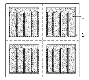
[0037] a) as attached figure 1 , 2 As shown, a p-type GaN layer 3, an active region 4, and an n-type GaN layer 5 are sequentially deposited on the epitaxial wafer of the sapphire substrate 6. After the chip is divided, the n-type GaN layer 5 is exposed in each chip unit to prepare chip electrodes. , to complete the sapphire wafer production;

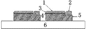
[0038] b) as attached image 3 , 4 As shown, wiring electrodes and interconnection lines are ...


PUM


Abstract

The invention discloses a high-power COB (Chip on Board)-packaged LED (Light Emitting Diode) structure. The high-power COB-packaged LED structure comprises a sub-mount, a wiring electrode, an interconnection circuit, a chip electrode, a p-type GaN layer, an active region, an n-type GaN layer and a fluorescent powder layer, wherein the sub-mount is positioned on a bottom layer; the wiring electrode and the interconnection circuit are formed on the sub-mount; the chip electrode corresponds to the wiring electrode; the p-type GaN layer, the active region and the n-type GaN layer are positioned above the chip electrode; the fluorescent powder layer is coated above the n-type GaN layer; and the wiring electrode and the chip electrode are bonded together. The manufacturing process is based on a chip flip technology and comprises the following steps: on the wafer level, bonding a p-type electrode and an n-type electrode of a high-power chip with corresponding p-type electrode and n-type electrode on the sub-mount; connecting integrated chips in series or in parallel by electrode arrangement of the sub-mount; stripping an original sapphire substrate; transferring the chips to the sub-mount; carrying out spin coating on a photosensitive fluorescent powder solvent on the sub-mount wafer and photoetching to form a shape-reserving fluorescent powder coating. The wafer-level COB-packaged LED structure is higher in production efficiency and quality; and the invention provides a realization method for further reducing the lumen cost of a CO package unit.

Description

technical field [0001] The invention relates to a high-power COB packaged LED structure and a manufacturing process thereof. Background technique [0002] Since LED packaging is one of the important determinants of device performance and accounts for a considerable proportion in device cost, reducing the cost per lumen has always been the main obstacle restricting the application of LEDs in the lighting field. In order to meet this market requirement, COB (chip-on-board) packaging has emerged in recent years. The so-called traditional high-power COB packaging usually refers to the packaging form in which multiple front-loading chips (die bonding) are fixed on a large-size packaging bracket, connected in series and parallel by wire bonding, coated with mixed phosphor silica gel, the phosphor naturally settles, and the silica gel is cured. Such encapsulation has the following disadvantages: [0003] 1. Since the bottom surface of the front-mounted chip is a sapphire substrat...

Claims


Application Information

Patent Timeline
IPC IPC(8): H01L33/48H01L33/64H01L33/62H01L33/50
CPCH01L2224/14
Inventor 李睿
Owner FOCUS LIGHTINGS SCI & TECH
Why Eureka
Try Eureka