A kind of field effect transistor and its manufacturing method

A field-effect transistor, polysilicon technology, applied in semiconductor/solid-state device manufacturing, semiconductor devices, electrical components, etc., can solve problems such as electrical parameter failure and leakage

Inactive Publication Date: 2015-12-16
PEKING UNIV FOUNDER GRP CO LTD +1
View PDF4 Cites 0 Cited by
  • Summary
  • Abstract
  • Description
  • Claims
  • Application Information

AI Technical Summary

Problems solved by technology

Due to the thin gate oxide layer, when its quality is not high, the gate and source can easily leak through the gate oxide layer, resulting in electrical parameter failure

Method used


Image

  • A kind of field effect transistor and its manufacturing method
  • A kind of field effect transistor and its manufacturing method
  • A kind of field effect transistor and its manufacturing method

Examples


Embodiment Construction

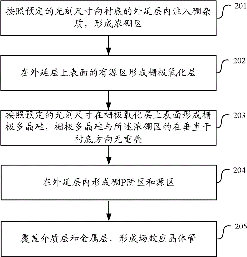
[0040] The embodiments of the present invention will be further described in detail below in conjunction with the accompanying drawings.

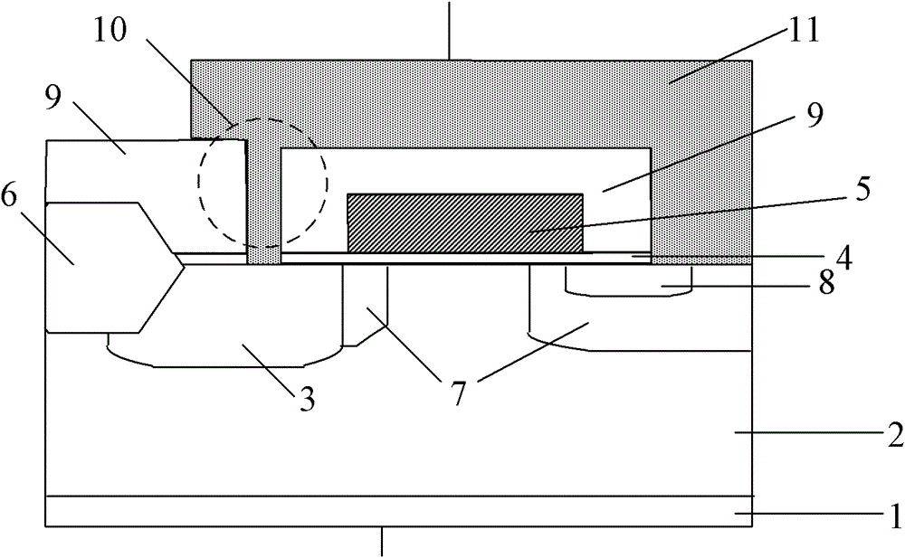
[0041] An embodiment of the present invention provides a field effect transistor, such as figure 1 As shown, the field effect transistor consists of:

[0042] an epitaxial layer 2 located on the upper surface of the substrate 1;

[0043] a boron-rich region 3 located in the epitaxial layer 2;

[0044] A gate oxide layer 4 located in the active region on the upper surface of the epitaxial layer 2;

[0045] Gate polysilicon 5 located on the upper surface of the gate oxide layer 4;

[0046] Wherein, the gate polysilicon 5 does not overlap with the boron-rich region 3 in a direction perpendicular to the substrate 2 .

[0047] Preferably, the field effect transistor further includes: a field oxide layer 6 located in the non-active area on the upper surface of the epitaxial layer 2 .

[0048] Preferably, the field effect transistor further i...


PUM


Abstract

The embodiment of the invention relates to the field of semiconductor technology, in particular to a field effect transistor and a manufacturing method thereof. The manufacturing method comprises the following steps: boron impurity is injected to an epitaxial layer of a substrate according to preset photoetching size to form a thick boron region; a gate oxide layer is formed in the active region of the upper surface of the epitaxial layer; gate polycrystalline silicon is formed on the upper surface of the gate oxide layer according to the preset photoetching size, and the gate polycrystalline silicon and the thick boron region are not superposed in the direction of being vertical to the substrate; and a boron P well region and a source region are formed in the epitaxial layer; and a dielectric layer and a metal layer are covered, and the field effect transistor is formed. With the adoption of the field effect transistor and a manufacturing method thereof, provided by the embodiment of the invention, through ensuring that the thick boron region and the gate polycrystalline silicon does not coincide, the gate-source leakage is avoided from being generated between the gate and the source through the boron impurity heavily-doped part of the gate oxide layer, so that the gate-source leakage probability of products is reduced.

Description

technical field [0001] The invention relates to the technical field of semiconductors, in particular to a field effect transistor and a manufacturing method thereof. Background technique [0002] Metal-oxide-semiconductor field-effect transistor MOSFET is a common voltage-driven device with three electrodes, namely gate, source, and drain. Its working principle is: the source is grounded, the drain is connected to the power supply potential, and through The on and off of the gate voltage controls the on and off of the current between the drain and the source. [0003] The vertical double-diffused metal oxide semiconductor transistor VDMOS is a kind of MOSFET. It forms a channel through the lateral difference of the two diffusions of the P well and the source region. Because the current direction of the VDMOS flows vertically from the drain on the back to the front, it can generate high current. density, it is widely used in power semiconductor applications. Hundreds of tho...

Claims


Application Information

Patent Timeline
Patent Type & Authority Patents(China)
IPC IPC(8): H01L29/06H01L29/78H01L21/027H01L21/336
Inventor 方绍明
Owner PEKING UNIV FOUNDER GRP CO LTD
Why Eureka
Try Eureka