
Modeling method for optical proximity correction process model

A technology of optical proximity effect and process model, which is applied in the field of modeling of optical proximity effect correction process model, can solve the problems of exposure capability gap, unscientific, different observers, etc., to ensure accuracy, reliability and stability, speed up fitting and Convergence time and effect of reducing the amount of measurement data

Inactive Publication Date: 2013-01-30
SHANGHAI HUAHONG GRACE SEMICON MFG CORP
View PDF3 Cites 7 Cited by
  • Summary
  • Abstract
  • Description
  • Claims
  • Application Information

AI Technical Summary

Problems solved by technology

Therefore, the existing method may lead to different judgments by different observers due to individual subjective reasons; at the same time, for critical dimensions below certain design rules, the existing method of visual judgment is even more unscientific
There is also a considerable gap between the exposure capability of the lithography machine calculated by the theoretical formula and the exposure capability of the actual machine; and when collecting OPC data, it is impossible to collect FEM (Focus Energy Matrix) for the key dimensions of each lithography. Determine the lithography process window for these critical dimensions

Method used


Image

  • Modeling method for optical proximity correction process model
  • Modeling method for optical proximity correction process model
  • Modeling method for optical proximity correction process model

Examples


Embodiment Construction

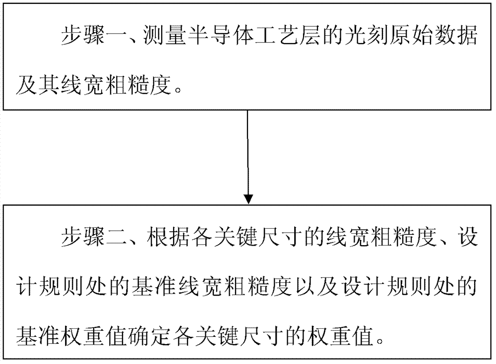
[0023] Such as figure 1 Shown is the flowchart of the method of the embodiment of the present invention. The modeling method of the optical proximity effect correction process model in the embodiment of the present invention includes steps:

[0024] Step 1. Using a scanning electron microscope to measure the lithography raw data of the semiconductor process layer and the line width roughness of the lithography raw data; the lithography raw data includes the measured values ​​of multiple key dimensions; the lithography raw data The line width roughness includes the line width roughness for each of the critical dimension measurements.

[0025] Step 2. Determine each key dimension according to the line width roughness of the measured value of each critical dimension, the reference line width roughness at the design rule of the semiconductor process layer, and the reference weight value at the design rule of the semiconductor process layer. The weight value of the key dimension...


PUM


Abstract

The invention discloses a modeling method for an optical proximity correction process model. The method comprises the steps of measuring original data and line width roughness of a semiconductor process layer; and determining weighted values of all critical sizes according to the line width roughness of the measured value of each critical size, a datum line width roughness at design rule checking position of the semiconductor process layer and a datum weighted value at the design rule checking position of the semiconductor process layer. By introducing the line width roughness to determine the weighted values of all the critical sizes, to-be-measured data can be reduced; some unstable factors and random factors of process, measuring machines and measuring processes can be filtered; fitting time and convergence time of the process model establishment can be shortened; and simultaneously accuracy and reliable stability of the process model can be guaranteed.

Description

technical field [0001] The invention relates to a semiconductor integrated circuit manufacturing process method, in particular to a modeling method of an optical proximity correction (Optical Proximity Correction, OPC) process model. Background technique [0002] In the existing Optical Proximity Correction (OPC, Optical Proximity Correction) process, a large amount of lithography raw data needs to be collected to establish a process model, and the process model includes a post-lithography process model or a post-etching process model. The method of collecting a large amount of lithography raw data in the modeling method of the existing optical proximity effect correction process model is: for each feature pattern, use different exposure units on the same silicon wafer to measure its lithography critical dimension. , CD), and then take the average value of the critical dimension as the original data of each lithography; this acquisition method is used to avoid large measurem...

Claims


Application Information

Patent Timeline
IPC IPC(8): G03F1/36
Inventor 陈福成袁春雨
Owner SHANGHAI HUAHONG GRACE SEMICON MFG CORP
Learn More