Manufacture method of semiconductor device

A manufacturing method and semiconductor technology, applied in the fields of semiconductor/solid-state device manufacturing, semiconductor devices, electric solid-state devices, etc., can solve problems such as indeterminacy, and achieve the effects of preventing the introduction of thermal strain, prolonging failure life, and high reliability.

Active Publication Date: 2012-12-26
FUJI ELECTRIC CO LTD
View PDF9 Cites 1 Cited by
  • Summary
  • Abstract
  • Description
  • Claims
  • Application Information

AI Technical Summary

Problems solved by technology

[0011] As for the structure of the semiconductor device 200, it cannot be determined uniformly from the structure of the module and the materials used for the position that causes failure during high-temperature operation.

Method used


Image

  • Manufacture method of semiconductor device
  • Manufacture method of semiconductor device
  • Manufacture method of semiconductor device

Examples


Embodiment Construction

[0064] Embodiments are illustrated in the following examples.

[0065]

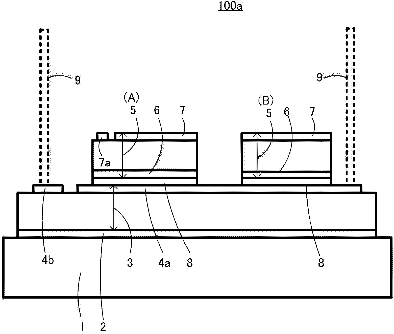
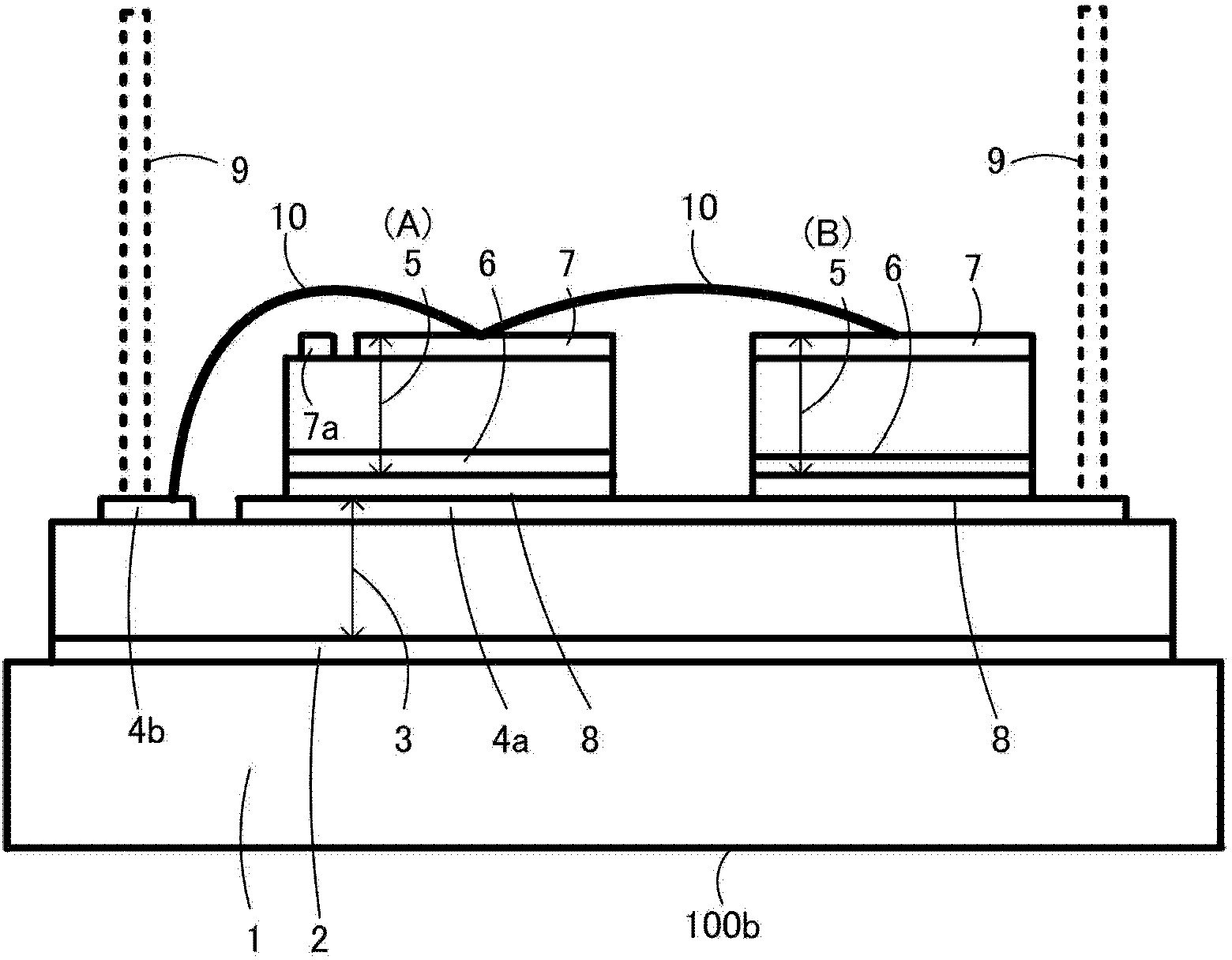
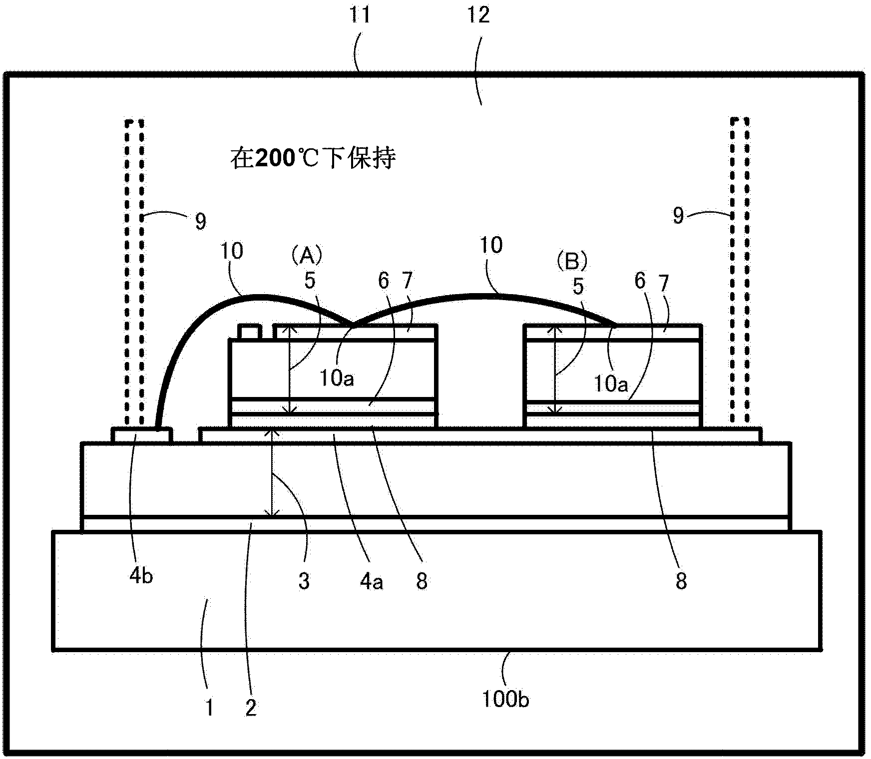
[0066] Figure 1 to Figure 6 This is a method of manufacturing a semiconductor device according to an embodiment of the present invention, and is a cross-sectional view of a main part of the manufacturing process shown in step by step. The semiconductor device is, for example, a power module in which an IGBT chip and a diode are connected in antiparallel.

[0067] First, if figure 1 As shown, the back electrode 6 of the semiconductor chip 5 is fixed with the bonding material 8 on the conductive pattern 4 a of the insulating substrate 3 with the conductive pattern 3 on which the bonding material 2 is fixed on the heat dissipation base plate 1 . In addition, an external lead-out terminal 9 is fixed to the conductive pattern 4b. This component composed of the heat dissipation base plate 1 , the insulating substrate with conductive patterns 3 , the semiconductor chip 5 and the external lead-out terminal...


PUM

PropertyMeasurementUnit
thicknessaaaaaaaaaa

Abstract

The invention provides a manufacture method of a semiconductor device, which can improve the reliability of a surface electrode of a semiconductor chip and a contact part of a metal wire by making the cooling speed from thermal aging treatment temperature proper. An aluminum wire (10) added with Ni is bonded on an Al-Si electrode film (surface electrode 7) of the semiconductor chip (5), the thermal aging treatment is performed at a high temperature belong 300 DEG C, and then the semiconductor device is gradually cooled according to the cooling speed below 1 DEG C/min, thus the process stress during the bonding process is removed, and the thermal stress guided by cooling after thermal aging treatment is suppressed, therefore the high reliability semiconductor device (100) is provided.

Description

technical field [0001] The invention relates to a method for manufacturing a semiconductor device, in particular to a method for bonding metal wires to surface electrodes of a semiconductor chip. Background technique [0002] In recent years, there has been a demand for downsizing and weight reduction of automotive instrument control devices and electric vehicle drive control devices. The drive control device uses a semiconductor device that switches a large current at high speed in order to obtain AC (power) for driving the motor from a DC power source such as a battery. In response to the increase in electric power, that is, the increase in the operating current of electronic components, aluminum is mainly used in the electrical connection between semiconductor chips in semiconductor devices, between semiconductor chips and insulating substrates with conductive patterns that are fastened to semiconductor chips, etc. Composition of tinsel. [0003] Such semiconductor devi...

Claims


Application Information

Patent Timeline
Patent Type & Authority Applications(China)
IPC IPC(8): H01L21/60
CPCH01L2224/45124H01L2224/48137H01L2224/73265H01L2224/78313H01L2224/85181H01L2224/7855H01L2924/12032H01L2924/1305H01L2924/13055H01L2924/13091H01L2224/32225H01L2224/48091H01L2224/48139H01L2224/48227H01L2224/92247H01L2224/06181H01L2224/0603H01L2224/85H01L2224/78H01L2924/00014H01L2924/00H01L2924/00012
Inventor 外园洋昭酒井茂西村知紘
Owner FUJI ELECTRIC CO LTD
Why Eureka
Try Eureka