Switch circuit capable of quickly discharging transistor parasitic capacitance charge and charge discharging method thereof
A parasitic capacitance and switching circuit technology, applied in the field of switch control circuits, can solve the problem of proportional damage of twice the delay time, and achieve the effects of reducing time overhead, reducing load startup delay time, and eliminating delay phenomenon.
- Summary
- Abstract
- Description
- Claims
- Application Information
AI Technical Summary
Problems solved by technology
Method used
Image
Examples
Embodiment 1
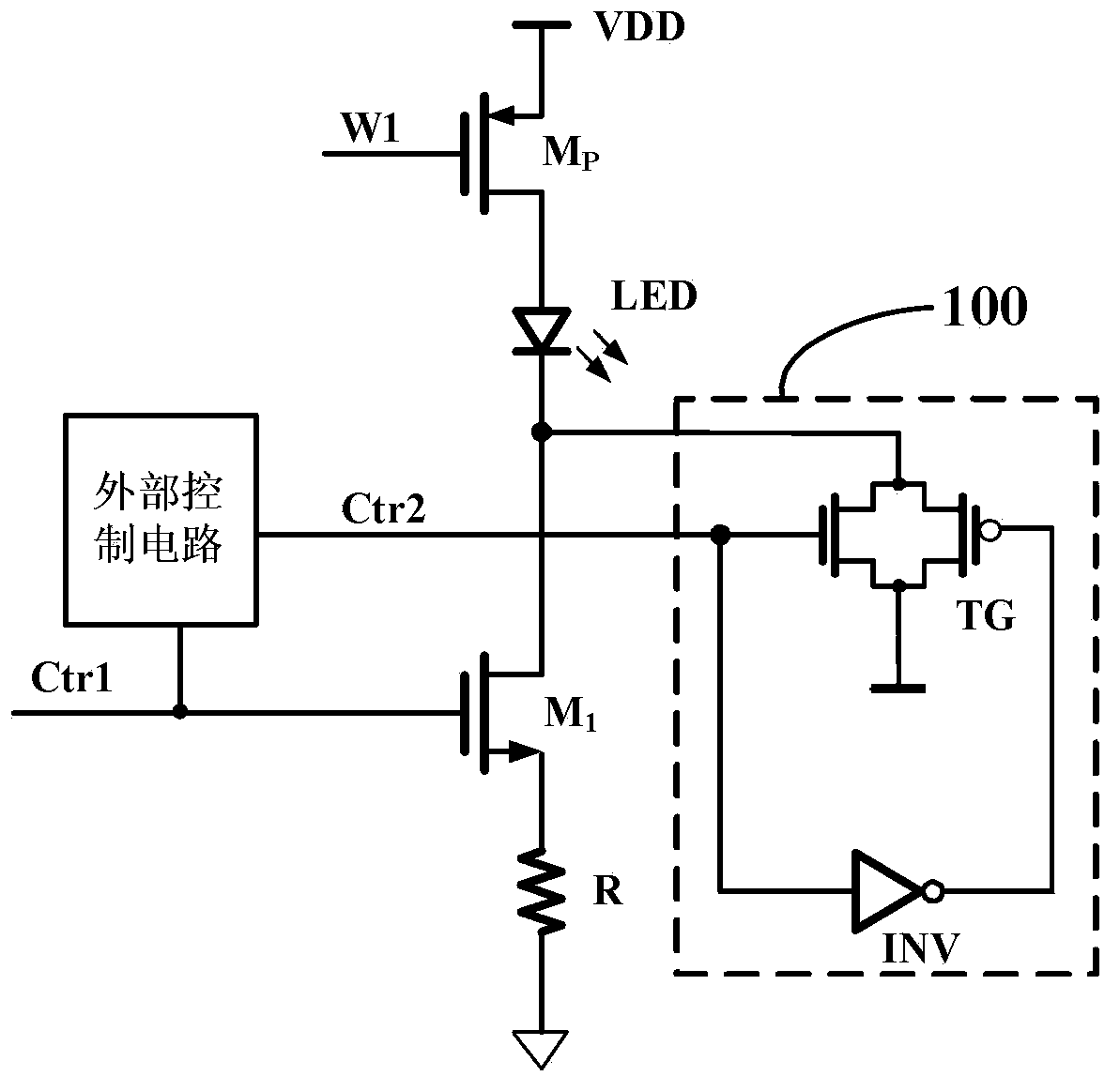
[0049] Such as figure 2 As shown, a switch circuit with a fast discharge transistor parasitic capacitance charge, including: NMOS tube M connected to the LED 1 , a resistor R and a charge discharge circuit 100 .
[0050] NMOS tube M 1 The drain of the LED is connected to the cathode of the LED and the input end of the charge discharge circuit 100, and the anode of the LED is connected through the PMOS transistor M p Connect to supply voltage V DD , NMOS tube M 1 The source of the resistor R is connected to one end of the resistor R, the other end of the resistor R is grounded, and the output terminal of the charge discharge circuit 100 is connected to a reference potential;
[0051] NMOS tube M 1 The gate of the gate receives the control signal Ctr1 provided by the external device, and the external control circuit provides the control signal Ctr2 to the control terminal of the charge discharge circuit 100 according to the state of the control signal Ctr1.
[0052] The c...
Embodiment 2
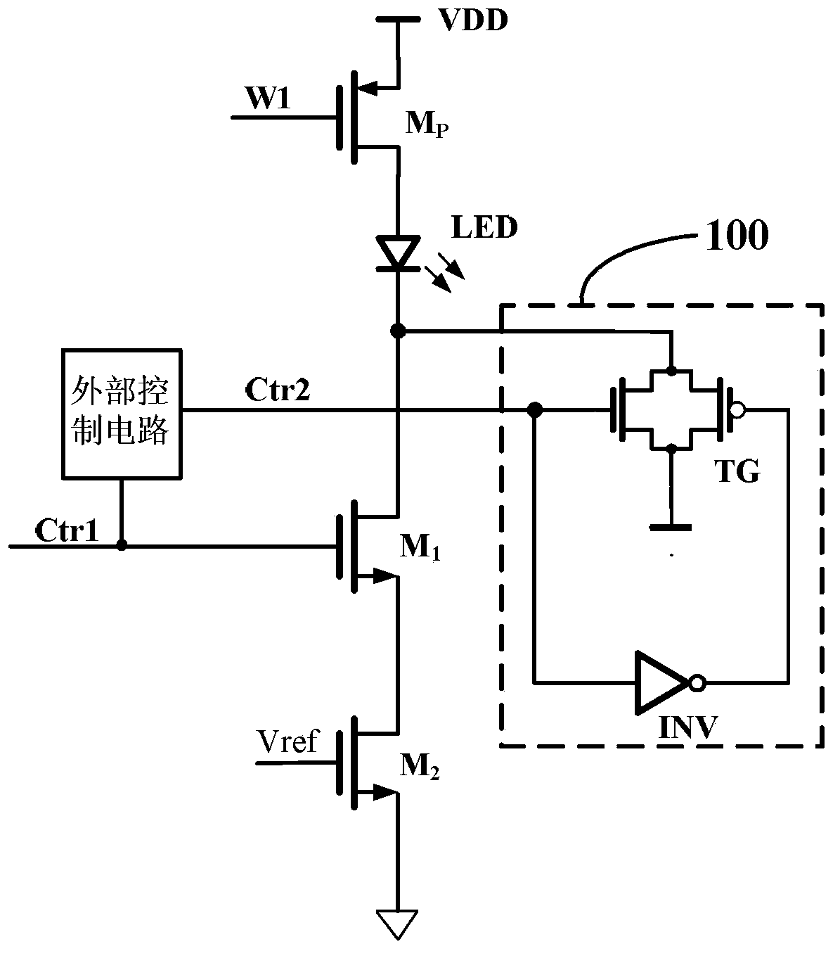
[0056] Such as image 3 As shown, a switch circuit with a fast discharge transistor parasitic capacitance charge, including: NMOS tube M connected to the LED 1 , NMOS tube M 2 and the charge discharge circuit 100.
[0057] NMOS tube M 1 The drain of the LED is connected to the cathode of the LED and the input end of the charge discharge circuit 100, and the anode of the LED is connected through the PMOS transistor M p Connect to supply voltage V DD , NMOS tube M 1 The source and NMOS tube M 2 The drain is connected, the NMOS tube M 2 The source of the charge discharge circuit 100 is connected to the reference potential, and the NMOS transistor M 2 The gate receives a given reference voltage signal V ref ;
[0058] NMOS tube M 1 The gate of the gate receives the control signal Ctr1 provided by the external device, and the external control circuit provides the control signal Ctr2 to the control terminal of the charge discharge circuit 100 according to the state of the ...
Embodiment 3
[0063] Such as Figure 4 As shown, a switch circuit with a fast discharge transistor parasitic capacitance charge, including: NMOS tube M connected to the LED 1 and the charge discharge circuit 100.
[0064] NMOS tube M 1 The drain of the LED is connected to the cathode of the LED and the input end of the charge discharge circuit 100, and the anode of the LED is connected through the PMOS transistor M p Connect to supply voltage V DD , NMOS tube M 1 The source of the charge discharge circuit 100 is connected to the reference potential;
[0065] NMOS tube M 1 The gate of the gate receives the control signal Ctr1 provided by the external device, and the external control circuit provides the control signal Ctr2 to the control terminal of the charge discharge circuit 100 according to the control signal Ctr1.
[0066] The charge discharge circuit 100 is composed of an NMOS transistor M N Composition; M N The drain of is the input end of the charge discharge circuit 100, M ...
PUM
 Abstract
Description
Claims
Application Information
 - R&D Engineer
- R&D Manager
- IP Professional
- Industry Leading Data Capabilities
- Powerful AI technology
- Patent DNA Extraction
Browse by: Latest US Patents, China's latest patents, Technical Efficacy Thesaurus, Application Domain, Technology Topic, Popular Technical Reports.
© 2024 PatSnap. All rights reserved.Legal|Privacy policy|Modern Slavery Act Transparency Statement|Sitemap|About US| Contact US: help@patsnap.com


