Welding structure for LED (light-emitting diode) array and circuit board thereof

A technology of LED array and welding structure, which is applied in the direction of printed circuit connected with non-printed electrical components, printed circuit components, electrical connection printed components, etc. Unable to power on and other problems, to achieve the effect of improving reliability, stable and reliable electrical connection, and reducing the probability of occurrence

Inactive Publication Date: 2012-11-14
AU OPTRONICS (XIAMEN) CORP +1
View PDF0 Cites 3 Cited by
  • Summary
  • Abstract
  • Description
  • Claims
  • Application Information

AI Technical Summary

Problems solved by technology

When the power line is at a certain angle to the PCB, it is easy to cause the pad to separate from the PCB board or the power line to detach from the pad, resulting in the failure of the PCB to be powered on, which in turn affects the work of the LED backlight of the backlight module.

Method used


Image

  • Welding structure for LED (light-emitting diode) array and circuit board thereof
  • Welding structure for LED (light-emitting diode) array and circuit board thereof
  • Welding structure for LED (light-emitting diode) array and circuit board thereof

Examples


Embodiment Construction

[0020] In order to make the technical content disclosed in this application more detailed and complete, reference may be made to the accompanying drawings and the following various specific embodiments of the present invention. The same signs in the accompanying drawings represent the same or similar components. However, those of ordinary skill in the art should understand that the embodiments provided below are not intended to limit the scope of the present invention. In addition, the drawings are only for illustrative purposes, and are not drawn according to their original dimensions.

[0021] The specific implementation manners of each aspect of the present invention will be further described in detail below with reference to the accompanying drawings.

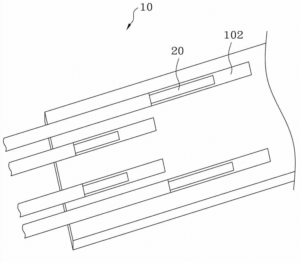
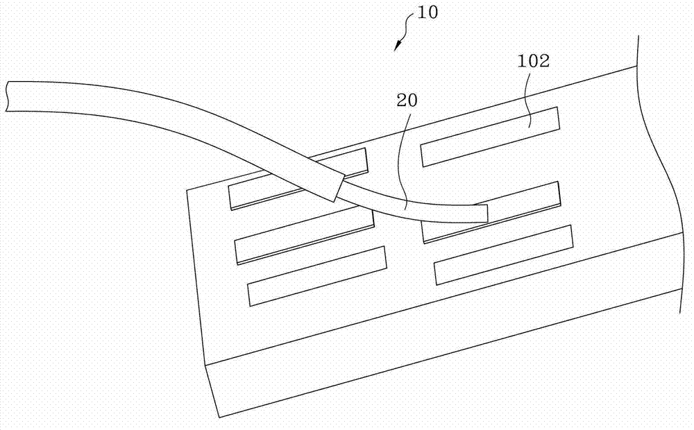
[0022] Figure 1A It shows a schematic diagram of a soldering structure in the prior art that uses a surface mount method to electrically connect an external power cord to a circuit board. Figure 1B show Figure 1A A schematic di...


PUM


Abstract

The invention provides a welding structure for an LED (light-emitting diode) array and a circuit board thereof. The welding structure comprises at least one welding hole, wherein the welding hole penetrates through a first surface and a second surface of the circuit board, the welding hole forms a first aperture on the first surface and forms a second aperture on the second surface, and the first aperture is smaller than the second aperture. According to the welding structure disclosed by the invention, the first aperture formed by the welding hole on the first surface of the circuit board is smaller than the second aperture formed on the second surface of the circuit board, so that the inner section of the welding hole is shaped like a trapezoid or the like, and when a power cord is inserted into the welding hole, the electrical connection between the power cord and the welding hole is more stable and more reliable in comparison with the surface-mounting connection way in the prior art. In addition, action force required for separating the power cord from a PCB (printed circuit board) can be increased by a soldering tin part and a sealing adhesive part on the inner section of the welding hole, so that the incidence of separating the power cord from the PCB can be reduced, and the working reliability of a backlight module can be enhanced.

Description

Technical field [0001] The invention relates to a welding structure, in particular to a welding structure for an LED array and its circuit board. Background technique [0002] The Back Light Module is one of the key components of the LCD panel. Since the liquid crystal itself does not emit light, the function of the backlight module is mainly to provide a light source with sufficient brightness and uniform distribution for the liquid crystal panel so that it can display images normally. Among them, the backlight can be a cold cathode fluorescent tube (CCFL, Cold Cathode Fluorescent Lamp), a hot cathode fluorescent tube, a light emitting diode (LED, Light Emitting Diode), etc. Compare LED backlight with CCFL backlight. Compared with traditional CCFL backlight, LED backlight has the characteristics of low power consumption, low heat generation, high brightness and long life span, and has gradually become the mainstream of the market. [0003] In the prior art, the LED backlight is ...

Claims


Application Information

Patent Timeline
Patent Type & Authority Applications(China)
IPC IPC(8): H05K1/18H05K1/11
Inventor 李振峰
Owner AU OPTRONICS (XIAMEN) CORP
Why Eureka
Try Eureka