Method for preparing graphene devices

A graphene and device technology, applied in the field of graphene optical lithography device preparation, can solve the problems of low time efficiency, high cost of electron beam exposure technology, unsuitable for large-scale production, etc., and achieve high production efficiency and good repeatability , Simple and controllable process conditions

Active Publication Date: 2012-10-24
PEKING UNIV
View PDF5 Cites 3 Cited by
  • Summary
  • Abstract
  • Description
  • Claims
  • Application Information

AI Technical Summary

Problems solved by technology

[0002] Graphene is a hot spot in nano-science research. Although graphene has been used to prepare various electrical and optical devices in the laboratory, the preparation methods of these devices are mainly based on the patterning technology of electron beam exposure. Although Good device performance can be obtained in the laboratory, but the electron beam lithography technique is costly, time inefficient and not suitable for mass production

Method used


Image

  • Method for preparing graphene devices
  • Method for preparing graphene devices
  • Method for preparing graphene devices

Examples


Embodiment Construction

[0026] Below in conjunction with the accompanying drawings, the present invention will be further described in detail through examples, but the present invention is not limited in any way.

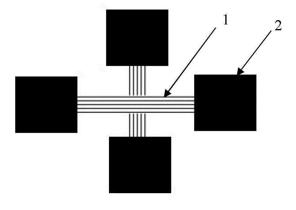
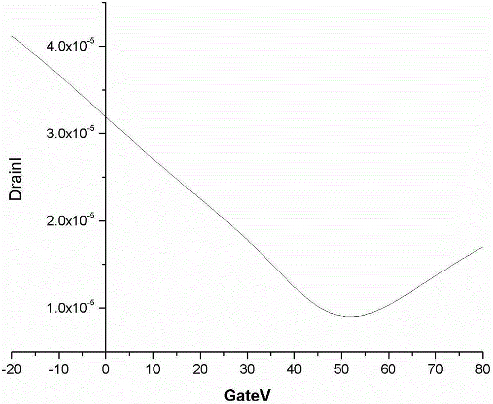
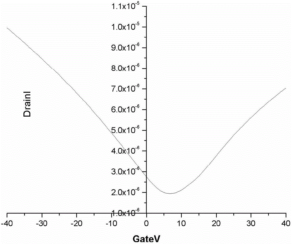
[0027] Such as figure 1 In the graphene lithography device shown, the graphene material as the active region is cross-shaped, the channel 1 is 10 microns long and 2 microns wide, and four electrodes 2 are in contact with the graphene channel 1, and the electrode material is For Ti / Au, you can choose two electrodes and add a bottom gate voltage for field effect measurement. Both the metal layer and the etching layer are patterned using Fuji I-line adhesive 665D. The specific preparation steps of the device are as follows:

[0028] 1. Grow graphene on the metal by chemical vapor deposition, and then transfer the graphene to the insulating substrate;

[0029] 2. The first optical lithography defines the pattern of the electrode on the insulating substrate, and then uses electron beam evapor...


PUM


Abstract

The invention discloses a method for preparing graphene devices. After graphene materials are photoetched, the impacts of the photoetching process on the performances of graphene are eliminated through chemical treatment with chlorobenzene and an adhesive remover AR 300-70, and the Dirac point and channel resistance of graphene can be controlled. The method is simple, can be used for producing the graphene devices in batches and greatly improves the processing efficiency and does not damage the excellent performances of graphene.

Description

technical field [0001] The invention relates to a method for preparing a graphene optical lithography device, in particular to a method for manufacturing a device on graphene with an optical lithography method and controlling the performance of the graphene device through chemical treatment. Background technique [0002] Graphene is a hot spot in nano-science research. Although graphene has been used to prepare various electrical and optical devices in the laboratory, the preparation methods of these devices are mainly based on the patterning technology of electron beam exposure. Although Good device performance can be obtained in the laboratory, but the electron beam lithography technique is costly, time inefficient and not suitable for mass production. In the current integrated circuit industry, optical lithography is the most commonly used and very mature patterning technology, and the development of optical lithography technology has always been the core driving force fo...

Claims


Application Information

Patent Timeline
IPC IPC(8): H01L21/04B82Y10/00G03F7/00
Inventor 石润伯徐慧龙张志勇彭练矛王胜
Owner PEKING UNIV
Why Eureka
Try Eureka