Liquid crystal device and projection-type display device

A technology for liquid crystal devices and image display areas, applied in projection devices, static indicators, optics, etc., can solve the problems of spread and the inability of peripheral electrodes to be placed in appropriate positions, to prevent the degradation of display quality and improve flatness. Effect

Inactive Publication Date: 2012-10-17
SEIKO EPSON CORP
View PDF1 Cites 3 Cited by
  • Summary
  • Abstract
  • Description
  • Claims
  • Application Information

AI Technical Summary

Problems solved by technology

[0006] However, since the dummy pixel electrodes are provided in the peripheral area through the conductive film of the same layer as the pixel electrodes, the level difference between the image display area and the peripheral area is eased to achieve flattening in the image display area, and there is a problem that it is impossible to describe in The problem that the peripheral electrode for trapping ionic impurities in Patent Document 1 is arranged at an appropriate position
For example, if the peripheral electrode for trapping ionic impurities is provided inside the region where the dummy pixel electrode is provided, the distance between the peripheral electrode and the image display region becomes too short, and the influence of the ionic impurities trapped in the peripheral electrode will spread to in the image display area

Method used


Image

  • Liquid crystal device and projection-type display device
  • Liquid crystal device and projection-type display device
  • Liquid crystal device and projection-type display device

Examples


Embodiment approach 1

[0030] (overall composition)

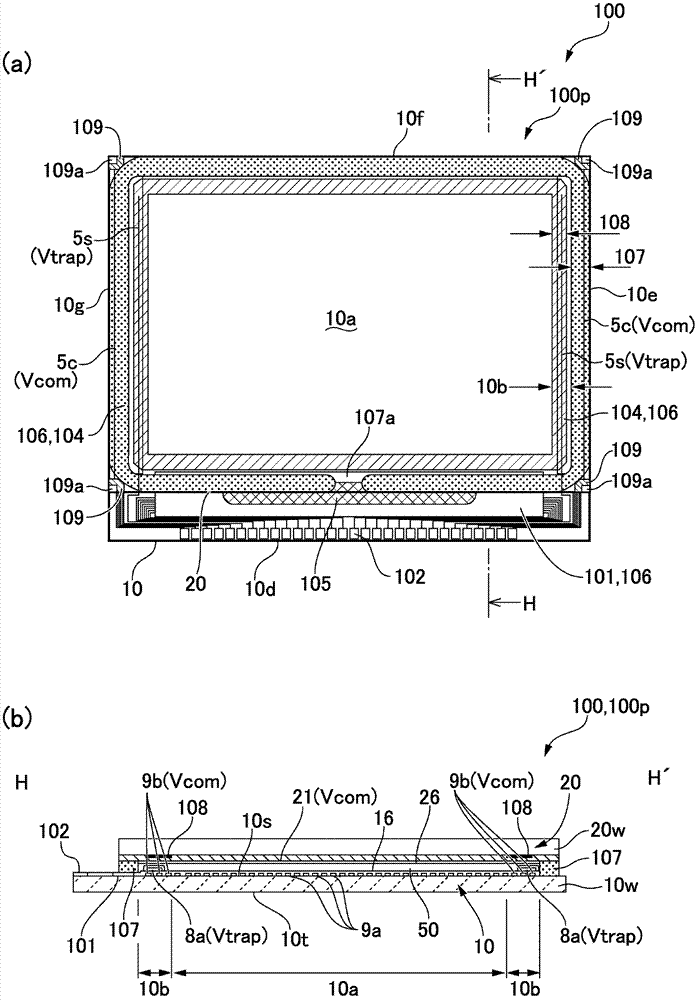
[0031] figure 1 It is a block diagram showing the electrical configuration of a liquid crystal device to which the present invention is applied. exist figure 1 Among them, the liquid crystal device 100 has a TN (Twisted Nematic, twisted nematic) mode and / or a VA (Vertical Alignment, vertical alignment) mode liquid crystal panel 100p, and the liquid crystal panel 100p has a plurality of pixels 100a arranged in a matrix in its central region. The image display area 10a. In the liquid crystal panel 100p, an element substrate 10 (refer to figure 2 etc.), a plurality of data lines 6a and a plurality of scanning lines 3a extend vertically and horizontally inside the image display area 10a, and pixels 100a are formed at positions corresponding to their intersections. In each of the plurality of pixels 100a, a pixel transistor 30 including a field effect transistor and a pixel electrode 9a described later are formed. The source of the pixel trans...

Embodiment approach 2

[0079] Figure 7 It is an explanatory diagram of the peripheral electrode 8a formed on the element substrate 10 of the liquid crystal device 100 according to Embodiment 2 of the present invention, Figure 7 (a) and (b) are explanatory diagrams which show the layout of the whole peripheral electrode 8a, and explanatory diagram which enlarged the peripheral electrode 8a. In addition, since the basic structure of this embodiment is the same as that of Embodiment 1, the same code|symbol is attached|subjected to a common part, and their description is abbreviate|omitted.

[0080] as shown in Figure 7 In other words, the liquid crystal device 100 of this embodiment is similar to the first embodiment, and the element substrate 10 also has an image display region 10a in which a plurality of pixel electrodes 9a are arranged and a peripheral region 10b sandwiched between the image display region 10a and the sealing material 107. . Further, in the peripheral region 10b, a part of the...


PUM


Abstract

In at least one embodiment of the disclosure, a liquid crystal device comprises a plurality of conductive patterns formed of a conductive film in a peripheral region between an image display region and a sealing member. The conductive patterns are formed at a same layer as a plurality of pixel electrodes. An insulation film is formed on a side facing a counter substrate so as to correspond to the plurality of conductive patterns and a plurality of pixel electrodes. Peripheral electrodes are formed in a region overlapping the plurality of conductive patterns in a plan view on a side on which the counter substrate is located so as to correspond to the insulation film in the peripheral region.

Description

technical field [0001] The present invention relates to a liquid crystal device holding liquid crystal between a pair of substrates, and a projection display device using the liquid crystal device as a light valve. Background technique [0002] In the liquid crystal device, an element substrate having an image display area in which a plurality of pixel electrodes are arranged on one side of the element substrate and a counter substrate provided with a common electrode to which a common potential is applied is provided with a sealing material, The liquid crystal layer is held in a region surrounded by the sealing material between the element substrate and the counter substrate. Such a liquid crystal device can be used as a light valve of a direct view display device and / or a projection display device. [0003] In such a liquid crystal device, if the ionic impurities mixed in when the liquid crystal is injected and / or the ionic impurities precipitated (eluted) from the sealin...

Claims


Application Information

Patent Timeline
Patent Type & Authority Applications(China)
IPC IPC(8): G02F1/1343G02F1/133G02F1/1337G09G3/36G03B21/14
CPCG02F1/1337G02F1/1343G09G2320/043G02F2201/501G02F1/133G02F2001/133388G09G2300/0417G09G3/002G02F1/133345G09G3/36G09G3/3648G09G2310/0232G02F1/133388
Inventor 横田智己原弘幸
Owner SEIKO EPSON CORP
Why Eureka
Try Eureka