Method for identifying semiconductor nano structure pattern
A nanostructure and semiconductor technology, applied in the direction of optical devices, instruments, measuring devices, etc., can solve the problems of lack of generalization ability, classification and recognition accuracy can not be guaranteed, and achieve the effect of high-precision feature shape recognition
- Summary
- Abstract
- Description
- Claims
- Application Information
AI Technical Summary
Problems solved by technology
Method used
Image

Examples
Embodiment Construction
[0026] The present invention is described in more detail below by means of examples, but the following examples are only illustrative, and the protection scope of the present invention is not limited by these examples.
[0027] This example takes a nanostructure as an example to illustrate the specific implementation steps of the present invention as follows:
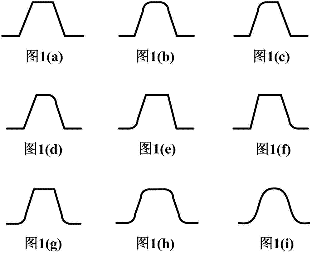
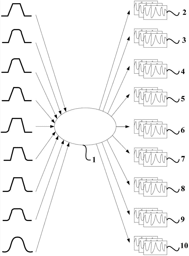
[0028] (1) Determining several different morphological features that may appear due to uncontrollable factors on the manufacturing process line of a nanostructure; assign a unique representative number to the analyzed nine nanostructures with different morphological features ;
[0029] figure 1 It is a schematic diagram of several different topographic features that may appear due to uncontrollable factors on the manufacturing process line of a one-dimensional trapezoidal periodic grating. figure 1 (a) is the nanostructure morphology expected to be produced in the process production, figure 1 (b)~ figure 1 (i) is an...
PUM
 Abstract
Description
Claims
Application Information
 - Generate Ideas
- Intellectual Property
- Life Sciences
- Materials
- Tech Scout
- Unparalleled Data Quality
- Higher Quality Content
- 60% Fewer Hallucinations
Browse by: Latest US Patents, China's latest patents, Technical Efficacy Thesaurus, Application Domain, Technology Topic, Popular Technical Reports.
© 2025 PatSnap. All rights reserved.Legal|Privacy policy|Modern Slavery Act Transparency Statement|Sitemap|About US| Contact US: help@patsnap.com