
Hollow lead-free plastic flat package

A cavity-free, flat package technology, applied in electrical components, electrical solid devices, circuits, etc., can solve the problems that MEMS chips and optoelectronic semiconductor chips cannot be plastic-packed, and achieve mass production, shorten the length of bonding wires, low cost effect

Inactive Publication Date: 2012-10-03
THE 13TH RES INST OF CHINA ELECTRONICS TECH GRP CORP
View PDF4 Cites 2 Cited by
  • Summary
  • Abstract
  • Description
  • Claims
  • Application Information

AI Technical Summary

Problems solved by technology

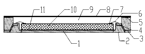
[0008] The technical problem to be solved by the present invention is to provide a cavity leadless plastic flat package, which solves the problem that MEMS chips with exposed movable structures and optoelectronic semiconductor chips cannot be plastic-packaged, and reduces the stress of the package, ensuring that the chip Reliability and safety of use

Method used


Image

  • Hollow lead-free plastic flat package
  • Hollow lead-free plastic flat package
  • Hollow lead-free plastic flat package

Examples


Embodiment Construction

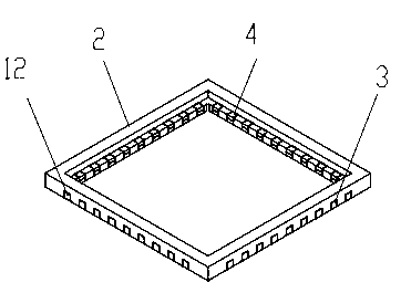
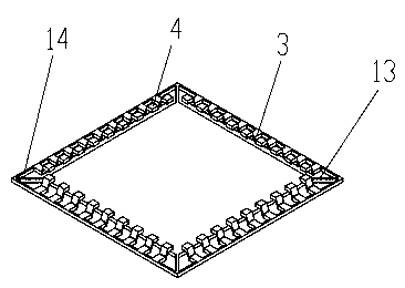
[0023] According to attached figure 1 It can be seen that the present invention specifically relates to a cavity leadless plastic flat package, including a carrier 1, on which a chip 10 is fixed, and pins are evenly distributed around the carrier 1, between the pins and between the pins and the carrier. Filling through the plastic package 2, the plastic package 2 bonds the pins and the carrier 1 into one, the plastic package 2 is an insulating material, and can be filled by injection molding.

[0024] According to attached figure 2 It can be seen that the pins and the chip 10 are connected through the bonding wire 6, and the top of the chip 10 is provided with a cover plate 8, and the periphery of the cover plate 8 is supported by the plastic package body 2, and the connection between the cover plate 8, the carrier 1 and the plastic package body 2 A cavity 9 is formed between them, and a MEMS chip with an exposed movable structure is placed in the cavity 9, which is the main...


PUM


Abstract

The invention discloses a hollow lead-free plastic flat package, belonging to the technical field of semiconductor packages. The hollow lead-free plastic flat package comprises a carrier, wherein a chip is fixed on the carrier, pins are uniformly distributed around the carrier, plastic package bodies are filled among the pins as well as between the pins and the carrier, the pins and chip are connected by bonding lines, a cover plate is arranged above the chip, the periphery of the cover plate is supported by the plastic package bodies, and a cavity is formed among the cover plate, the carrier and the plastic package bodies. The hollow lead-free plastic flat package solves the problem that an MEMS (Micro Electro Mechanical System) chip with an exposed movable structure and a photoelectric semiconductor chip are incapable of being subjected to plastic package and reduces the packaging stress.

Description

technical field [0001] The invention relates to a semiconductor flat package, which belongs to the technical field of semiconductor packaging, in particular to a cavity leadless plastic flat package. Background technique [0002] The semiconductor package is a bridge between the semiconductor chip and the peripheral electronic and electrical system. It is not only the mechanical support and protection structure of the semiconductor chip, but also provides power and signal paths for the connection between the semiconductor chip and the peripheral electronic circuit. heat dissipation channel. In the semiconductor industry chain, semiconductor packaging and testing is one of the three pillars alongside design and manufacturing. [0003] Semiconductor packaging mainly includes metal packaging, ceramic packaging, metal ceramic packaging and plastic packaging. Metal packaging is a hermetic package, usually using traditional metal processing methods to process the material into a...

Claims


Application Information

Patent Timeline
Patent Type & Authority Applications(China)
IPC IPC(8): H01L23/02H01L23/04H01L23/49
CPCH01L2224/48091H01L2224/73265H01L2224/48247H01L2924/1461H01L2924/00014H01L2924/00
Inventor 徐爱东许鹏杨拥军
Owner THE 13TH RES INST OF CHINA ELECTRONICS TECH GRP CORP
Learn More