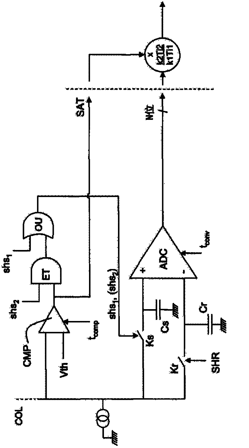
Image sensor with very high dynamics
A kind of technology of image sensor and sensor, applied in the field of image sensor
- Summary
- Abstract
- Description
- Claims
- Application Information
AI Technical Summary
Problems solved by technology
Method used
Image
Examples
Embodiment Construction
[0027] exist figure 1 The main components of an example CMOS technology active pixel including electron multiplying amplification structures are depicted in .
[0028] The pixel is formed in a substrate 10, and the substrate 10 preferably includes a P-type lightly doped semiconductor active layer 12 (the symbol P- is used to indicate this weak doping), and the P-type lightly doped semiconductor active layer 12 is formed on a further at the surface of the heavily doped layer (P+). A pixel is isolated from adjacent pixels by an insulating barrier 13, which completely surrounds the pixel. The barrier layer may be an isolation trench above the P-well.
[0029] The pixel includes a photodiode region PHD whose perimeter follows the contour of the N-type semiconductor region implanted in the portion of the depth of the active layer 12 . This implanted region is topped by a P+ type surface region 16 which is held at zero reference potential. This is a so-called "pinned" photodiode...
PUM
 Abstract
Description
Claims
Application Information
 - R&D
- Intellectual Property
- Life Sciences
- Materials
- Tech Scout
- Unparalleled Data Quality
- Higher Quality Content
- 60% Fewer Hallucinations
Browse by: Latest US Patents, China's latest patents, Technical Efficacy Thesaurus, Application Domain, Technology Topic, Popular Technical Reports.
© 2025 PatSnap. All rights reserved.Legal|Privacy policy|Modern Slavery Act Transparency Statement|Sitemap|About US| Contact US: help@patsnap.com


