Semiconductor integrated circuit and receiving apparatus
A technology of integrated circuits and semiconductors, applied in electrical components, impedance matching networks, transmission systems, etc., and can solve the problems of deterioration of noise characteristics of analog circuits, difficulty in low-voltage operation, and increased installation costs.
- Summary
- Abstract
- Description
- Claims
- Application Information
AI Technical Summary
Problems solved by technology
Method used
Image

Examples
no. 1 Embodiment
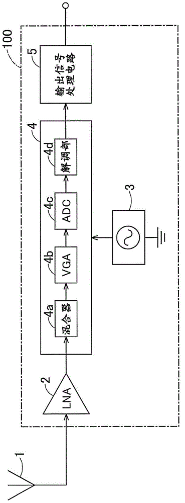
[0031] figure 1 It is a schematic block diagram of the receiving apparatus 100 of the first embodiment. The receiving device 100 includes an LNA (semiconductor integrated circuit) 2, a LO (Local Oscillator: local oscillator) signal generating unit 3, a demodulation circuit 4, and an output signal processing circuit 5. The receiving device 100 is mounted on, for example, a wireless LAN (Local Area Network) device, and processes the radio wave signal received by the antenna 1 and outputs it to the outside.
[0032] LNA2 amplifies the radio wave signal received by antenna 1. The LO signal generating unit 3 generates an LO signal that serves as a reference for the demodulated radio wave signal. The frequency of the LO signal is 2.5 GHz, for example. The demodulation circuit 4 demodulates the amplified radio wave signal based on the LO signal. More specifically, the demodulation circuit 4 includes a mixer 4a, a VGA (Variable Gain Amplifier) 4b, an ADC (Analog to Digital Converter...
no. 2 Embodiment
[0082] The first embodiment described above is provided with an impedance adjusting section having a fixed impedance value. On the other hand, in the second embodiment described below, an impedance adjusting section with variable impedance is provided.
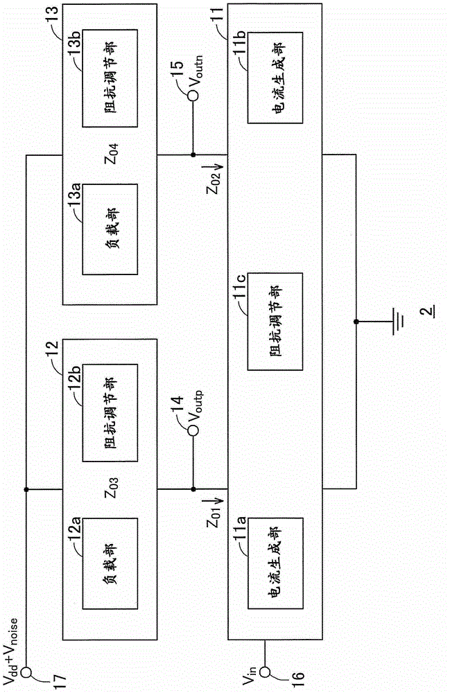
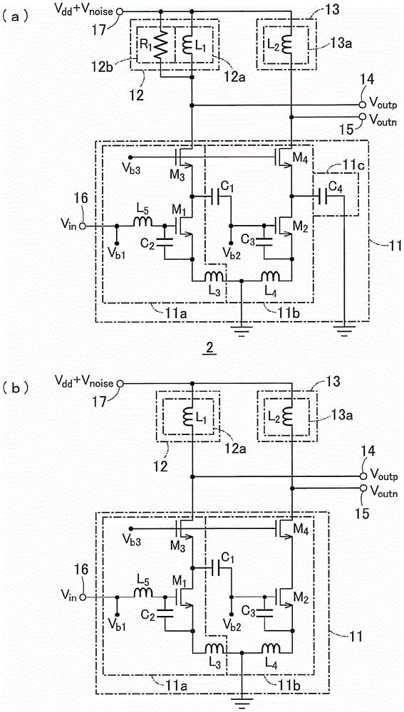
[0083] Picture 11 It is a schematic block diagram of an example of the internal structure of the LNA 21 of the second embodiment. Picture 11 In, and figure 2 The same components are given the same symbols, and the following description focuses on the differences.
[0084] The control signals V1 to V3 are input to the impedance adjustment sections 111c, 121b, and 131b of the LNA 21, respectively. By the control signals V1 to V3, the impedance of the impedance adjusting parts 111c, 121b, and 131b can be variably controlled. versus figure 2 Similarly, at least one of the transconductance circuit 111 and the load circuits 121 and 131 may have an impedance adjustment unit to which a control signal is input.
[0085] Even if the impe...
no. 3 Embodiment
[0099] The third embodiment automatically sets the control signal in the second embodiment.
[0100] Figure 19 It is a schematic block diagram of the receiving apparatus 101 of the third embodiment. Figure 19 In, and figure 1 The same components are given the same symbols, and the following description focuses on the differences.
[0101] Figure 19 The receiving device 101 further includes a detection circuit 6 and a control circuit 7. In addition, LNA21 such as Picture 11 As shown, there is at least one impedance adjusting part that variably controls impedance according to a control signal. The detection circuit 6 detects degradation of the output signal of the output signal processing circuit 5. The control circuit 7 sets the control signal of the LNA 21 to suppress the deterioration of the output signal.
[0102] The control circuit 7 sets all control signals to all values, for example, and finally sets the value that most suppresses the degradation of the output signal amon...
PUM
 Abstract
Description
Claims
Application Information
 - R&D
- Intellectual Property
- Life Sciences
- Materials
- Tech Scout
- Unparalleled Data Quality
- Higher Quality Content
- 60% Fewer Hallucinations
Browse by: Latest US Patents, China's latest patents, Technical Efficacy Thesaurus, Application Domain, Technology Topic, Popular Technical Reports.
© 2025 PatSnap. All rights reserved.Legal|Privacy policy|Modern Slavery Act Transparency Statement|Sitemap|About US| Contact US: help@patsnap.com