Manufacturing method of pixel structure
A manufacturing method and pixel structure technology, which is applied in semiconductor/solid-state device manufacturing, electrical components, circuits, etc., can solve problems such as inability to meet users, complicated process, and inability to reduce production cost and output rate.
- Summary
- Abstract
- Description
- Claims
- Application Information
AI Technical Summary
Problems solved by technology
Method used
Image

Examples
Embodiment Construction
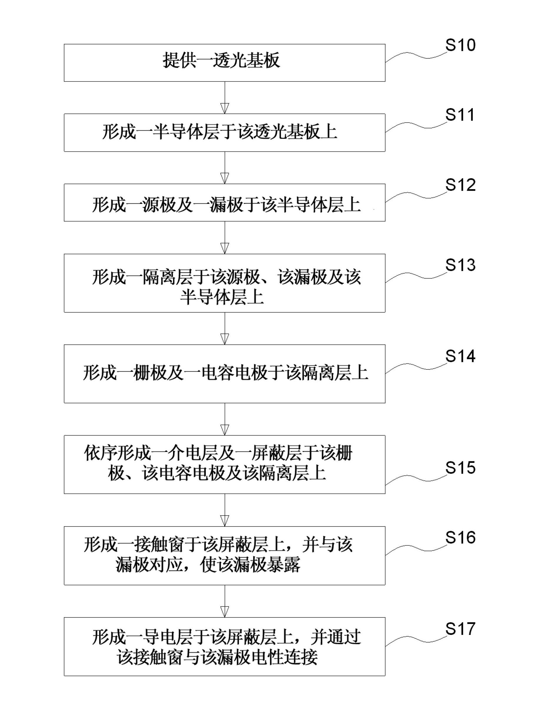
[0064] In order to enable your examiner to have a further understanding and understanding of the structural features and achieved effects of the present invention, a description of preferred embodiments and diagrams are provided.
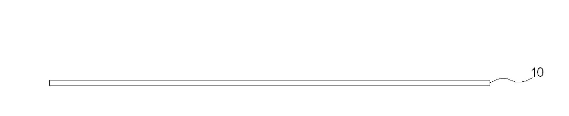
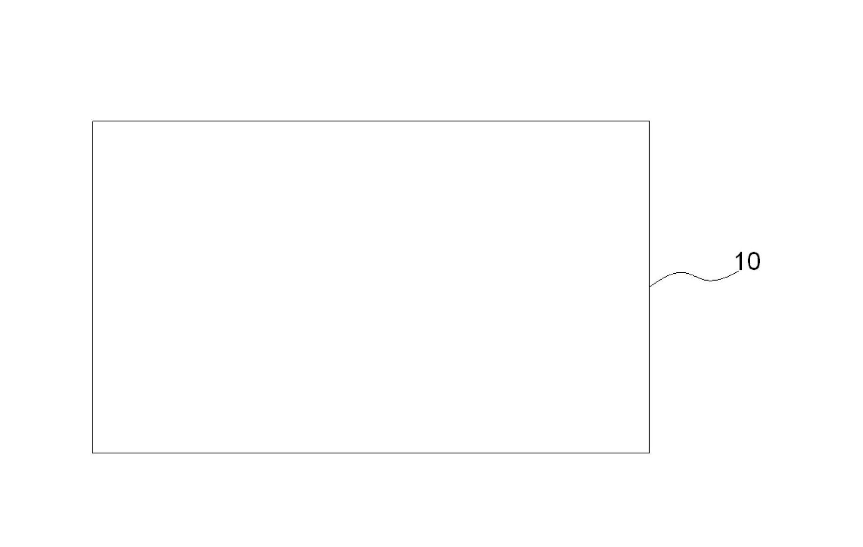
[0065] see figure 1 , Figure 2A and Figure 2B , are respectively a schematic diagram of the manufacturing process of the pixel structure of the present invention, a schematic cross-sectional structural diagram of step S10 of the present invention, and a schematic top view structural diagram of step S10 of the present invention. As shown in the figure: the present invention provides a thin film transistor and a pixel structure and a manufacturing method thereof. The manufacturing method of the pixel structure is to firstly perform step S10 to provide a light-transmitting substrate 10, and the material of the light-transmitting substrate 10 includes glass, quartz Or plastic, but depending on design requirements, the light-transmitting substrate 10...
PUM
 Abstract
Description
Claims
Application Information
 - R&D
- Intellectual Property
- Life Sciences
- Materials
- Tech Scout
- Unparalleled Data Quality
- Higher Quality Content
- 60% Fewer Hallucinations
Browse by: Latest US Patents, China's latest patents, Technical Efficacy Thesaurus, Application Domain, Technology Topic, Popular Technical Reports.
© 2025 PatSnap. All rights reserved.Legal|Privacy policy|Modern Slavery Act Transparency Statement|Sitemap|About US| Contact US: help@patsnap.com