
Image processing device and method as well as system

An image processing device and image signal processing technology, applied in image communication, TV system components, TV, etc., can solve the problems of poor image processing reliability and high image processing cost, and achieve the effect of ensuring reliability

Inactive Publication Date: 2012-08-08
HUNAN RAMON SCI & TECH
View PDF4 Cites 18 Cited by
  • Summary
  • Abstract
  • Description
  • Claims
  • Application Information

AI Technical Summary

Problems solved by technology

[0004] In view of this, an embodiment of the present invention provides an image processing device, method and system to solve the problems of high cost of image processing and poor reliability of image processing in the prior art

Method used


Image

  • Image processing device and method as well as system
  • Image processing device and method as well as system
  • Image processing device and method as well as system

Examples


Embodiment Construction

[0041] The technical solutions in the embodiments of the present invention will be clearly and completely described below in conjunction with the accompanying drawings in the embodiments of the present invention. Obviously, the described embodiments are only a part of the embodiments of the present invention, rather than all the embodiments. Based on the embodiments of the present invention, all other embodiments obtained by those of ordinary skill in the art without creative work shall fall within the protection scope of the present invention.

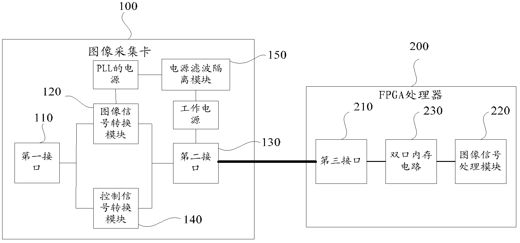
[0042] figure 1 It is a schematic diagram of the structure of an image processing device provided by an embodiment of the present invention, refer to figure 1 The image processing device includes: an image capture card 100 and an FPGA (Field-Programmable Gate Array) processor 200. The FPGA processor 200 is connected to the image capture card 100, and performs parallel processing on the image signals collected by the image capture card 100...


PUM


Abstract

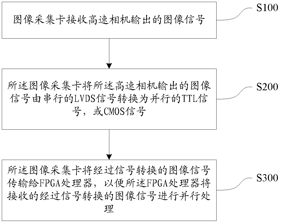
The embodiment of the invention provides an image processing device and method as well as system. The image processing device comprises an image acquisition card and a FPGA (Field Programmable Gate Array) processor; the image acquisition card comprises a first interface, an image signal conversion module and a second interface, wherein the first interface is used for receiving image signals output by a high-speed camera, the image signal conversion module is used for converting the image signals into parallel TTL (Transistor-Transistor Logic) signals or CMOS (Complementary Metal Oxide Semiconductor) signals from serial LVDS (Low Voltage Differential Signals), and the second interface is used for transmitting the image signals subjected to the signal conversion to the FPGA processor; and the FPGA processor comprises a third interface and an image signal processing module, wherein the third module is used for receiving the image signals which are transmitted by the second interface and are subjected to the signal conversion, and the image signal processing module is used for carrying out parallel processing on the received image signals. The image processing device solves the problem that the prior art is high in cost as multiple devices are adopted for processing the image signals, and simultaneously the image signals are processed in a hardware manner, thereby the reliability of the image signal processing is ensured.

Description

Technical field [0001] The present invention relates to the technical field of image acquisition and processing, and more specifically, to an image processing device, method and system. Background technique [0002] With the rapid development of machine vision technology, high-speed cameras represented by line scan cameras have been widely used. The signal output interface of high-speed cameras is mostly the standard Camera Link interface, and the signal output rate can reach Gbps (1Gbps is 1204 megabits per second). [0003] For the processing of the Gbps-level image signal output by the high-speed camera, the existing mainstream image signal processing methods are as follows: the image capture card supporting the high-speed camera captures the image signal output by the high-speed camera, and transmits the captured image signal to the host. It can be an industrial computer or a server, and the host performs subsequent image processing according to the preset image processing sof...

Claims


Application Information

Patent Timeline
Patent Type & Authority Applications(China)
IPC IPC(8): H04N5/14H04N5/77
Inventor 罗旗舞田陆
Owner HUNAN RAMON SCI & TECH
Learn More