
Realization device of column-level analog-to-digital converter (ADC) in complementary metal-oxide semiconductor (CMOS) image sensor

An image sensor, column-level technology, applied in the field of analog integrated circuit design, can solve the problems of short SAADC conversion cycle, increased design difficulty, long conversion cycle, etc.

Inactive Publication Date: 2012-07-25
TIANJIN UNIV
View PDF3 Cites 23 Cited by
  • Summary
  • Abstract
  • Description
  • Claims
  • Application Information

AI Technical Summary

Problems solved by technology

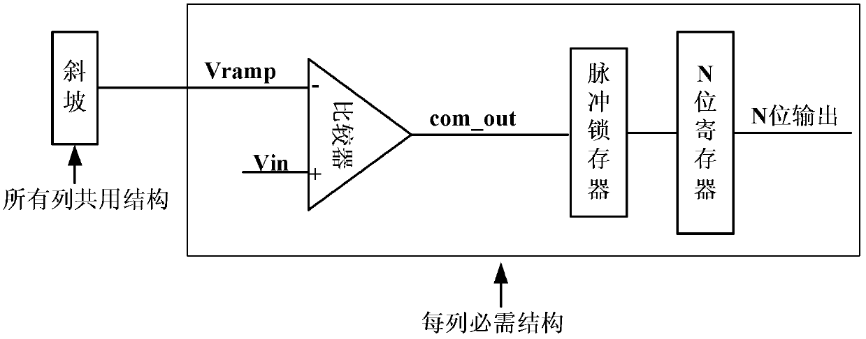
The disadvantage of SS ADC is long conversion cycle, N-bit SS ADC needs 2 N -1 clock cycle to complete a conversion
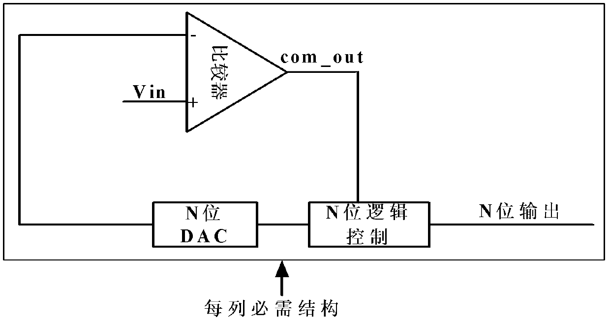
image 3 It is an N-bit SAADC circuit structure diagram. Compared with SS ADC, the conversion period of SA ADC is very short. N-bit SA ADC only needs N clock cycles to complete a conversion. Its disadvantage is that each column requires a complete N-bit ADC, so the layout area of ​​each column is very large, which increases the difficulty of design

Method used


Image

  • Realization device of column-level analog-to-digital converter (ADC) in complementary metal-oxide semiconductor (CMOS) image sensor
  • Realization device of column-level analog-to-digital converter (ADC) in complementary metal-oxide semiconductor (CMOS) image sensor
  • Realization device of column-level analog-to-digital converter (ADC) in complementary metal-oxide semiconductor (CMOS) image sensor

Examples


Embodiment Construction

[0018] by Figure 4 The scheme shown is an example. All columns share two ramps. The binary code value that generates ramp 1 is one bit more than the binary code value that generates ramp 2. The signals generated by ramp 1 and ramp 2 pass through the sample and hold circuit and the voltage buffer ( buffer) are respectively connected to the high and low reference voltages required by the DAC in the SA ADC of each column. The circuit structure required for each column is similar to SA ADC, but switches S4, S5, sampling capacitors C1, C2 and two buffers are added. There are two switches at the negative end of the comparator in each column. When performing high M-bit conversion, the negative terminal of the comparator is connected to the ramp signal generated by ramp 1; when performing low N-M bit conversion, the negative terminal is connected to the signal generated by the DAC in SAADC. So the SS ADC shares a comparator with the SAADC.

[0019] It works as follows:

[0020] Th...


PUM


Abstract

The invention relates to the field of analog integrated circuit design. In order to provide an analog-to-digital converter (ADC) structure which has a simple structure and a short conversion cycle, and achieve the purpose of improving the dynamic scope of a sensor, the technical adopts the following technical scheme that: a realization device of a column-level ADC in complementary metal-oxide semiconductor (CMOS) image sensor comprises a single-slope ADC, a successive approximation ADC and two slope signal generators; the single-slope ADC, the successive approximation ADC and a group of six switches form a unit, and each column in a sensor pixel array is provided with the unit; and two slope signal generators are shared by each column of the sensor pixel array. The realization device of the column-level ADC in the CMOS image sensor is mainly applied in the design and manufacturing of the semi-conductor image sensor.

Description

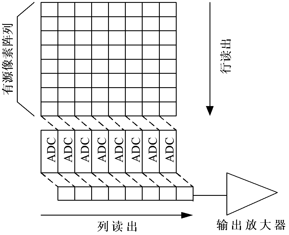
technical field [0001] The present invention relates to the field of analog integrated circuit design, in particular to a realization device of a column-level ADC applied in an image sensor, that is, a realization device of a column-level ADC in a CMOS image sensor. Background technique [0002] With the rapid development of digital technology and semiconductor manufacturing technology, CMOS image sensors have become the focus of current and future markets. Currently, there are three different types of analog-to-digital converters (ADCs) used in CMOS image sensors: pixel level, column level, and chip level. figure 1 It is a column-level ADC architecture diagram. Compared with chip-level ADC, column-level ADC has lower requirements on ADC speed, thus reducing chip power consumption and design difficulty. At the same time, compared with the pixel-level ADC, the column-level ADC is transferred from the inside of the pixel to the outside of the pixel array, which greatly improv...

Claims


Application Information

Patent Timeline
Patent Type & Authority Applications(China)
IPC IPC(8): H04N5/378H04N5/3745H03M1/38
Inventor 徐江涛徐文静姚素英高静史再峰聂凯明高岑
Owner TIANJIN UNIV
Learn More