Plane miniaturization communication band-pass filter with broadband external inhibition characteristic
A band-pass filter and filter technology, which is applied to waveguide devices, electrical components, circuits, etc., can solve the problem of electrical size reduction and achieve the effects of maintaining broadband out-of-band suppression, maintaining low loss, and small loss
- Summary
- Abstract
- Description
- Claims
- Application Information
AI Technical Summary
Problems solved by technology
Method used
Image
Examples
Embodiment 1
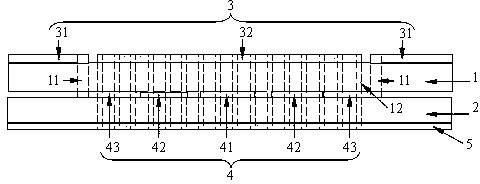
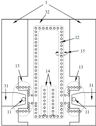
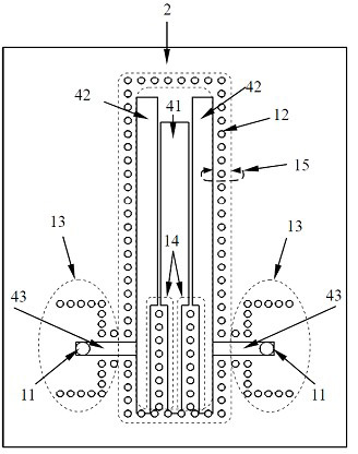
[0028] The filter structure is as figure 1 All dimensions shown are in mm. The size of the substrate in this embodiment is 19.8×24×1.13. The measured filter S-parameters and insertion loss results are shown in Figure 4 and Figure 5 .
[0029] The filter in this embodiment includes a filter part formed by using a substrate integrated coaxial line and a microstrip line for testing, and is realized by using three metal layers and two dielectric layers. The filter is composed of three quarter-wavelength substrate integrated coaxial resonators located in the middle metal layer. The resonators are directly coupled to the external input and output ports, and the coupling is coupled by adding isolation blind holes and changing the spacing between the resonators. The amount is controlled to achieve band-pass response and out-of-band rejection characteristics.
[0030] The center frequency of the filter in this embodiment is 2.35 GHz, and the corresponding insertion loss is 0.96...
PUM
 Abstract
Description
Claims
Application Information
 - R&D
- Intellectual Property
- Life Sciences
- Materials
- Tech Scout
- Unparalleled Data Quality
- Higher Quality Content
- 60% Fewer Hallucinations
Browse by: Latest US Patents, China's latest patents, Technical Efficacy Thesaurus, Application Domain, Technology Topic, Popular Technical Reports.
© 2025 PatSnap. All rights reserved.Legal|Privacy policy|Modern Slavery Act Transparency Statement|Sitemap|About US| Contact US: help@patsnap.com


