Optical films with controlled surface morphology and the method of manufacturing the same
An optical film and manufacturing method technology, applied in optics, optical components, optical components, etc., can solve the problems of large coating speed, maximum limit, air merging, etc., to achieve the effect of improving productivity
- Summary
- Abstract
- Description
- Claims
- Application Information
AI Technical Summary
Problems solved by technology
Method used
Image

Examples
Embodiment 1
[0051] Preparation of cellulose acylate solution
[0052] The composition described below was introduced into the mixer and dissolved therein at a temperature of 30°C:
[0053] Cellulose acetate 19wt%
[0054] Dichloromethane 73wt%
[0055] Methanol 6.0wt%
[0056] Triphenyl Phosphate 1.05wt%
[0057] Biphenyl diphenyl phosphate 0.5wt%
[0058] UV absorber 1 (benzotriazole cresol 328, Ciba (Ciba) company) 0.2wt%
[0059] UV absorber 2 (benzotriazole cresol 327, Ciba) 0.2wt%
[0060] SiO 2 0.05wt%
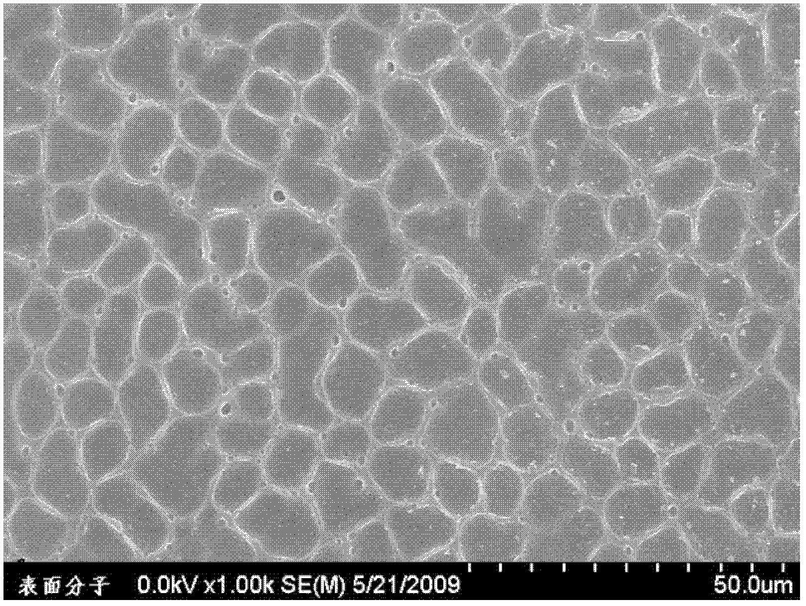
[0061] Cellulose acetate having a weight average molecular weight of 250,000 and a degree of substitution of 2.8 was used. The SiO used here 2 Has an average elementary particle diameter of about 20 nm. The resulting solution was conveyed by a gear pump, heated to 30° C., filtered through a filter paper with an absolute filtration accuracy of 0.01 mm, and then further filtered through a cartridge filter with an absolute filtration accuracy of 5 μm.
[0062] Production...
Embodiment 2
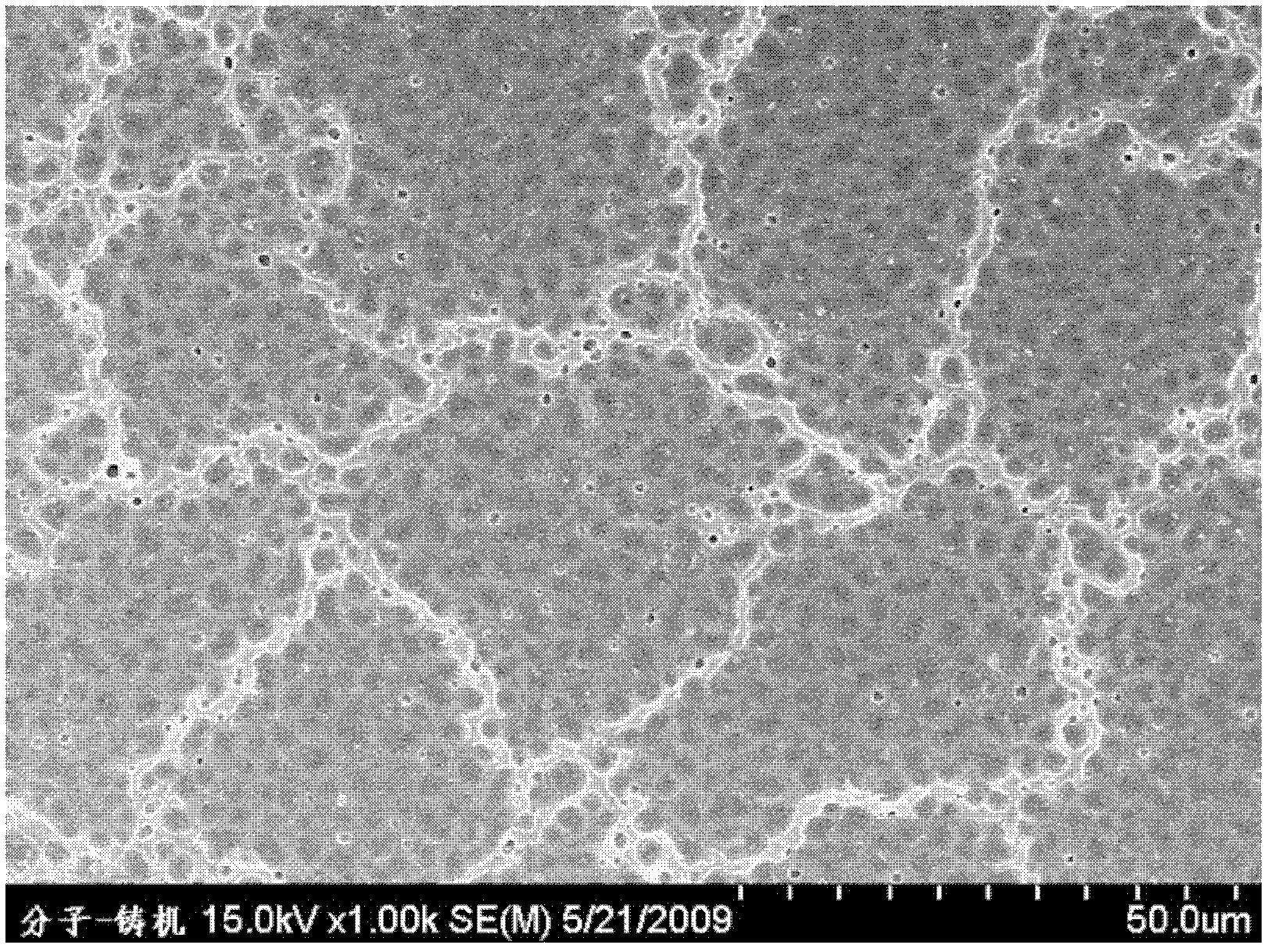
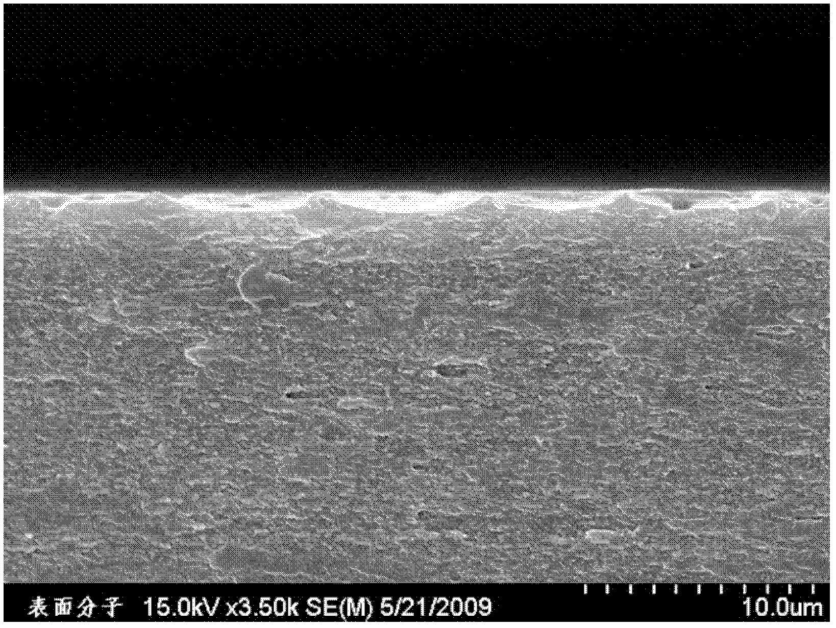
[0066] The film obtained from Example 1 was used to provide a film with a scratch resistant clear coating. A photocurable acrylic coating solution was coated on the Example 1 film. The coating solution had a binder solids content of 43 wt%, and included 42.2 wt% methyl ethyl ketone and 14.8 wt% isopropanol as solvents. The coating solution was coated using a No. 5 Mayer bar, dried in an oven at 100° C. for 30 seconds, and passed through a 57 mJ / cm 2 · s intensity of UV light for 10 seconds at 25°C. The dried and cured film exhibited a transparent appearance with a coating of about 5 μm thickness and 3H pencil hardness. The film has the physical properties listed in Table 1.
Embodiment 3
[0068] The same coating solution as in the Mayer rod coating experiment of Example 2 was used, and a cellulose acetate film with controlled surface morphology was used in a multiple coater to determine the coating speed at which bubble coalescence occurred. A slot die was used as a coating die and the drying temperature was individually controlled in three zones of 60°C, 100°C, and 110°C. To ensure the stability of the coating beads, vacuum suction was used. The film has the physical properties listed in Table 2.
PUM
| Property | Measurement | Unit |
|---|---|---|
| surface roughness | aaaaa | aaaaa |
| thickness | aaaaa | aaaaa |
| diameter | aaaaa | aaaaa |
Abstract
Description
Claims
Application Information
 - R&D
- Intellectual Property
- Life Sciences
- Materials
- Tech Scout
- Unparalleled Data Quality
- Higher Quality Content
- 60% Fewer Hallucinations
Browse by: Latest US Patents, China's latest patents, Technical Efficacy Thesaurus, Application Domain, Technology Topic, Popular Technical Reports.
© 2025 PatSnap. All rights reserved.Legal|Privacy policy|Modern Slavery Act Transparency Statement|Sitemap|About US| Contact US: help@patsnap.com