
Secondary deposition and dispersion process for selective emitter battery

A secondary deposition and diffusion process technology, applied in the direction of circuits, electrical components, climate sustainability, etc., can solve problems such as increasing the flow rate, failing to make batteries with selective emitter mechanisms, and prolonging the power-on time

Inactive Publication Date: 2012-07-11
YINGLI ENERGY CHINA
View PDF1 Cites 7 Cited by
  • Summary
  • Abstract
  • Description
  • Claims
  • Application Information

AI Technical Summary

Problems solved by technology

However, prolonging the power-on time or increasing the flow rate not only increases the overall cost of laser doping, but also fails to achieve the expected effect of making selective emitter mechanism batteries.

Method used


Image

  • Secondary deposition and dispersion process for selective emitter battery
  • Secondary deposition and dispersion process for selective emitter battery
  • Secondary deposition and dispersion process for selective emitter battery

Examples


Embodiment Construction

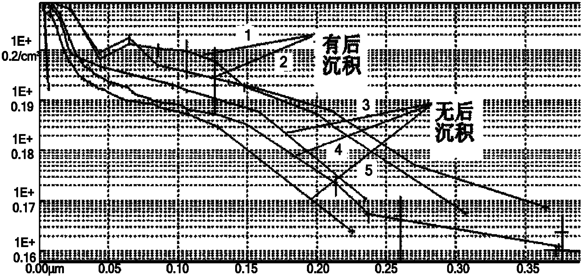
[0028] The invention discloses a secondary deposition and diffusion process for a selective emitter cell, so as to ensure sufficient phosphorus source concentration for laser doping technology and simultaneously ensure the surface quality of silicon wafers of crystalline silicon solar cells.

[0029] The technical solutions in the embodiments of the present invention will be clearly and completely described below in conjunction with the accompanying drawings in the embodiments of the present invention. Apparently, the described examples are only some examples of the present invention, not all embodiments. Based on the embodiments of the present invention, all other embodiments obtained by persons of ordinary skill in the art without making creative efforts fall within the protection scope of the present invention.

[0030] This embodiment provides a secondary deposition and diffusion process for selective emitter cells, which is used to deposit phosphorus sources on the surface...


PUM


Abstract

The invention provides a secondary deposition and dispersion process for a selective emitter battery. The secondary deposition and dispersion process is used for performing phosphorus source deposition on the surface of a crystalline silicon solar cell silicon slice, and comprises the following steps of: putting the crystalline silicon solar cell silicon slice into a first preset-temperature environment, and feeding a phosphorus source and oxygen until the phosphorus source is deposited to preset concentration, or putting the crystalline silicon solar cell silicon slice into a third preset-temperature environment, feeding the phosphorus source and the oxygen, and pushing the phosphorus source at first preset temperature until the phosphorus source is deposited to the preset concentration; and when the phosphorus source is deposited to the preset concentration, reducing the temperature to second preset temperature, continuing to feed the phosphorus source and the oxygen so as to perform phosphorus source deposition, and performing laser doping to obtain a crystalline silicon solar cell subjected to secondary deposition. After temperature reduction is performed, the phosphorus source and the oxygen are continued to be fed, so that the phosphorus source continues to be deposited on the surface of the silicon slice, and the concentration of the phosphorus source on the surface of the silicon slice is increased; a laser doping process is performed on the crystalline silicon solar cell silicon slice at relatively high phosphorus source concentration, so that relatively low laser energy can be adopted; and the required crystalline silicon solar cell can be obtained.

Description

technical field [0001] The invention relates to the technical field of solar cell preparation, in particular to a secondary deposition and diffusion process for selective emitter cells. Background technique [0002] Crystalline silicon is the most ideal material for solar cells, and crystalline silicon solar cells account for 90% of the photovoltaic market. The conversion efficiency of crystalline silicon solar cells is an important factor affecting its development. [0003] Realizing a selective emitter structure on crystalline silicon is one of the ways to improve the efficiency of crystalline silicon solar cells. The crystalline silicon solar cell with selective emitter structure uses a special process to form high and low P-N junctions on the surface of the silicon wafer of the crystalline silicon solar cell (hereinafter referred to as the silicon wafer). The selective emitter structure has two basic features, one is to form a highly doped deep diffusion region under t...

Claims


Application Information

Patent Timeline
IPC IPC(8): H01L31/18
CPCY02P70/50
Inventor 胡海波宋伟鹏范志东马桂艳史金超马红娜
Owner YINGLI ENERGY CHINA
Learn More