Flash memory unit forming method

A flash memory cell and substrate surface technology, which is applied in electrical components, semiconductor/solid-state device manufacturing, circuits, etc., can solve the problems of flash memory cell double peak effect, reverse narrow channel effect, transistor cycle durability and so on, so as to avoid double peak effect, improved cycle durability, and uniform thickness

Active Publication Date: 2015-04-29
SEMICONDUCTOR MANUFACTURING INTERNATIONAL (BEIJING) CORP
View PDF8 Cites 0 Cited by
  • Summary
  • Abstract
  • Description
  • Claims
  • Application Information

AI Technical Summary

Problems solved by technology

[0009] However, existing flash memory cells are prone to double peak effect and reverse narrow channel effect
In addition, the cycle durability of existing transistors is relatively poor

Method used


Image

  • Flash memory unit forming method
  • Flash memory unit forming method
  • Flash memory unit forming method

Examples


Embodiment Construction

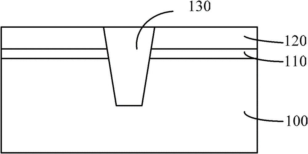
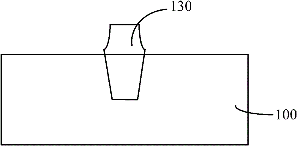
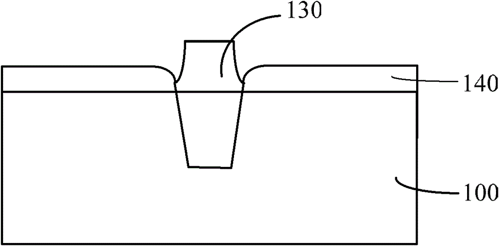
[0028] It can be known from the background technology that the flash memory cell formed by the existing flash memory cell forming method will produce a double peak effect and an inverse narrow channel effect, and the cycle durability of the flash memory cell is relatively poor. The inventors of the present invention have studied the above problems and tried to solve the above problems by adjusting the parameters of each step, but the results were very little. Therefore, the inventor further adjusted the process and found that the tunneling oxide was formed by a chemical vapor deposition process. Layer can solve the above problems.

[0029] According to the inventor's experimental research, a method for forming a flash memory cell is provided in the present invention. The method for forming a flash memory unit provided by the present invention includes: providing a substrate; forming a tunnel oxide layer on the surface of the substrate using a chemical vapor deposition method; and...


PUM


Abstract

A flash memory unit forming method comprises the steps as follows: a substrate is provided; a liner oxidation layer and an etching stop layer are formed sequentially on the surface of the substrate; at least two active areas are included in the substrate, and the adjacent active areas are isolated by a shallow trench isolation structure; the etching stop layer and the liner oxidation layer on the surface of the substrate are sequentially removed; a tunneling oxidation layer is formed on the surface of the substrate by a chemical vapor deposition method; and the tunneling oxidation layer is subjected to later stage oxidizing annealing treatment. The flash memory unit forming method provided by the invention avoids the double-hump effect and the reverse narrow channel effect, and the flash memory unit is better in period durability.

Description

Technical field [0001] The invention relates to the field of semiconductors, and in particular to a method for forming a flash memory unit. Background technique [0002] The standard physical structure of flash memory is called a flash memory unit (bit). The structure of the flash memory cell is different from conventional MOS transistors. The gate and conductive channel of a conventional MOS transistor are separated by a gate insulating layer, which is generally an oxide layer; while the flash memory has a control gate (CG: control gate, which is equivalent to the gate of a conventional MOS transistor). There is also a floating gate (FG: floating gate) between the pole and the conductive channel. Due to the existence of the floating gate, the flash memory can complete three basic operating modes: read, write, and erase. Even in the absence of power supply, the existence of the floating gate can maintain the integrity of the stored data. Adjacent flash memory cells are separa...

Claims


Application Information

Patent Timeline
Patent Type & Authority Patents(China)
IPC IPC(8): H01L21/336H01L21/28H01L21/285
Inventor 沈亿华宋化龙李亮史运泽涂火金
Owner SEMICONDUCTOR MANUFACTURING INTERNATIONAL (BEIJING) CORP
Why Eureka
Try Eureka