
A hybrid non-volatile flash memory and its storage system

A storage system and memory technology, applied in the field of memory, can solve the problems of no fusion of eNOR flash memory and NAND flash memory, complex system structure, low storage density, etc., and achieve large-capacity data storage capacity operation mode, flexible operation mode, and reduction The effect of small chip area

Inactive Publication Date: 2014-10-22
TSINGHUA UNIV
View PDF3 Cites 0 Cited by
  • Summary
  • Abstract
  • Description
  • Claims
  • Application Information

AI Technical Summary

Problems solved by technology

The disadvantage is that contact holes are required between adjacent storage units of eNOR flash memory, and some auxiliary read, write and erase logic is required, so its storage density is small and its capacity is small
In addition, the slow erasing and programming speed and large block size of eNOR flash memory make eNOR flash memory unsuitable for large-capacity data storage
[0005] Since NAND flash memory and eNOR flash memory have the above-mentioned complementary advantages and disadvantages, their application fields are different from each other and cannot replace each other.
Existing digital products using NAND flash memory and eNOR flash memory at the same time have the following problems: On the one hand, the process flow of NAND flash memory and eNOR flash memory is different, so they need to be produced separately, which increases the production cost of the product; NAND flash memory is An independent chip is integrated into the system, while eNOR flash memory is embedded in other circuit system chips. The different integration methods of the two lead to a larger system area, which affects the final size of the product; on the other hand, NAND flash memory is used as Large-capacity data storage medium, while eNOR flash memory is used as a small-capacity system program storage medium, and RAM (random access memory) is required as a data cache medium. Different storage systems are combined through multiple chip packages, resulting in the entire system complex structure
However, the ORNAND structure, like the OneNAND structure, cannot directly support the local code execution function, but must be executed through another NOR array or the ORNAND instruction code is downloaded to DRAM (Dynamic Random Access Memory) to run.
[0008] In summary, neither ORNAND nor OneNAND technology has truly integrated eNOR flash memory and NAND flash memory in essence.

Method used


Image

  • A hybrid non-volatile flash memory and its storage system
  • A hybrid non-volatile flash memory and its storage system
  • A hybrid non-volatile flash memory and its storage system

Examples


Embodiment Construction

[0030] Embodiments of the present invention are described in detail below, examples of which are shown in the drawings, wherein the same or similar reference numerals designate the same or similar elements or elements having the same or similar functions throughout. The embodiments described below by referring to the figures are exemplary only for explaining the present invention and should not be construed as limiting the present invention.

[0031] In describing the present invention, it should be understood that the terms "center", "longitudinal", "transverse", "upper", "lower", "front", "rear", "left", "right", " The orientations or positional relationships indicated by "vertical", "horizontal", "top", "bottom", "inner", "outer", etc. are based on the orientation or positional relationships shown in the drawings, and are only for the convenience of describing the present invention and simplifying Describes, but does not indicate or imply that the device or element referred...


PUM


Abstract

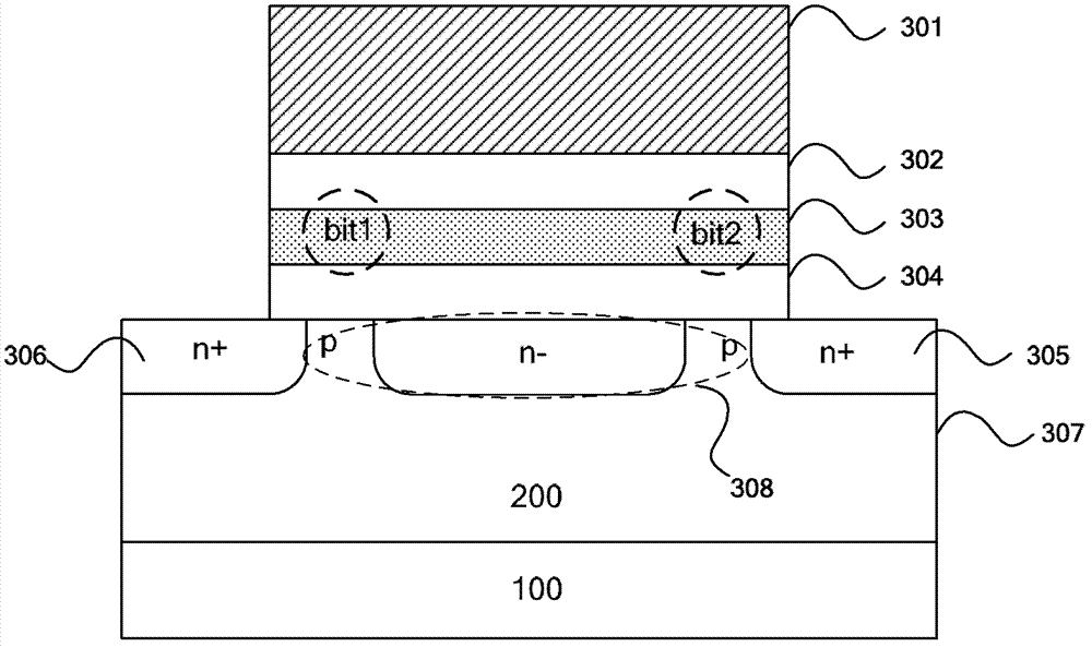
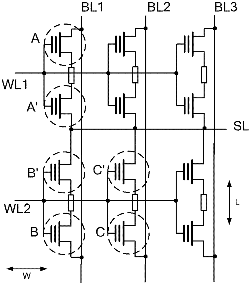
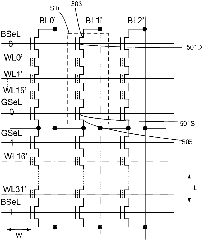
The invention provides a hybrid non-volatile flash memory. A memory unit of the memory including a gutter channel area positioned on a semiconductor substrate, a grid electrode positioned on the gutter channel area and a source end positioned in the semiconductor substrate at the first edge of the grid electrode and a drainage end positioned in the semiconductor substrate at the second edge of the grid electrode, wherein the grid electrode consists of a tunneling oxidizing layer, a silicon nitride layer, a blocking oxidizing layer and a polycrystalline silicon grid layer. In the embodiment of the invention, a double-bit non-uniform gutter channel device with high density serves as the memory unit, a NOR array and a NAND array are formed on the same chip through the double-bit non-uniform gutter channel device, single chip hybrid memory of an eNOR flash memory and a NAND flash memory is formed by utilizing the same process, so that high-capacity data storage of the NAND flash memory and quick program reading of the eNOR flash memory are realized through a smaller chip area.

Description

technical field [0001] The invention relates to the technical field of memory, in particular to a hybrid non-volatile flash memory and a storage system including the hybrid non-volatile flash memory. Background technique [0002] Flash memory (Flash) can be divided into NAND type and NOR type according to its different logical structure. [0003] NAND flash memory refers to the memory cells forming the entire array through a series relationship. Since there is no need for contact holes between adjacent memory cells, the equivalent area of ​​a single memory cell is small, and the structure density of the entire array is high. At the same time, the structure of the storage unit realizing the NAND structure is relatively simple, and the erasure is fast. The downside is that it is slower to read and does not support code-native execution. The characteristics of NAND flash memory determine that it is suitable for high-density and large-capacity data storage. [0004] NOR-type...

Claims


Application Information

Patent Timeline
Patent Type & Authority Patents(China)
IPC IPC(8): H01L27/115G11C16/04H10B69/00
Inventor 潘立阳刘利芳
Owner TSINGHUA UNIV
Learn More