System and method for carrying out configuration on memories
A memory and storage block technology, applied in the direction of memory address/allocation/relocation, input/output to record carrier, etc., can solve the problems of complex hardware structure and high configuration cost, and achieve less control logic, power saving, and flexibility high effect
- Summary
- Abstract
- Description
- Claims
- Application Information
AI Technical Summary
Problems solved by technology
Method used
Image
Examples
example 1
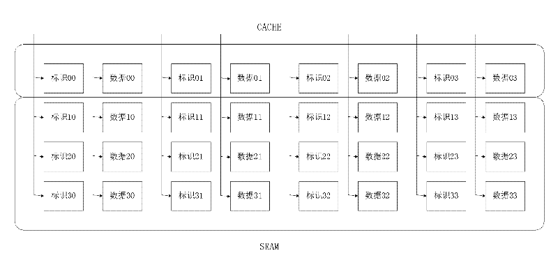
[0080] Example 1: In Figure 2a , assuming that the total size of the memory 110 is 256KB, and the ratio of Cache to SRAM is 1:3, then the size of Cache is 64KB. Assuming that the Cache is a four-way set associative, the size of each way is 16KB. If the size of each line of the Cache is 32B, each way of the Cache has 512 lines. Therefore, the size of the SRAM is 192KB, that is, 256KB−64KB=192KB.
[0081] In this case, the address of Cache is divided into:
[0082] 31 .. 14 13 .. 5 4 .. 2 1 .. 0 logo group address inline word address byte address
[0083] And, the address of SRAM is divided into:
[0084] 17 .. 16 15 .. 14 13 .. 5 4 .. 2 1 .. 0 row block address block address row address inline word address byte address
[0085] In this case, the row block address of the SRAM, that is, the 17:16 bits of the SRAM address, is only valid at 00, 01, and 10, and is invalid at 11, because the SRAM is not available at this ti...
example 2
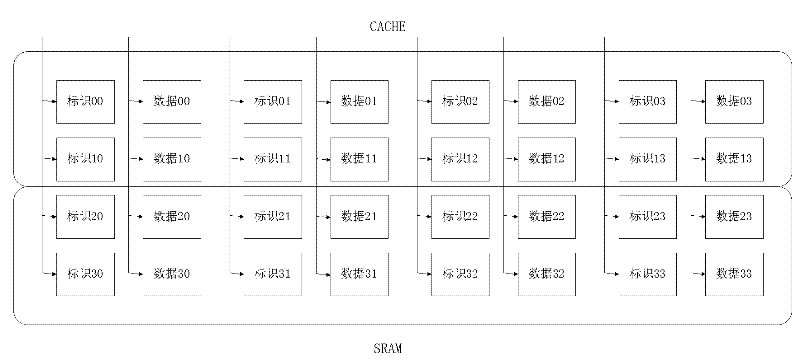
[0086] Example 2: In Figure 2b In the example, assuming that the total size of the memory 110 is 256KB, and the ratio of the Cache to the SRAM is 1:1, then the size of the Cache is 128KB. Assuming that the Cache is a four-way set associative, the size of each way is 32KB. If the size of each line of the Cache is 32B, then each way of the Cache has 1024 lines. The Cache may consist of two 16KB storage blocks. Therefore, the size of the SRAM is 128KB, that is, 256KB−128KB=128KB.
[0087] In this case, the address of Cache is divided into:
[0088] 31 .. 15 14 .. 5 4 .. 2 1 .. 0 logo Group No inline word offset byte offset
[0089] Among them, the 14th bit is used to select memory blocks of different rows. And, the address of SRAM is divided into:
[0090] 16 15 .. 14 13 .. 5 4 .. 2 1 .. 0 row block address block address row address inline word address byte address
[0091] When the memory 110 is configured as an SR...
PUM
 Abstract
Description
Claims
Application Information
 - Generate Ideas
- Intellectual Property
- Life Sciences
- Materials
- Tech Scout
- Unparalleled Data Quality
- Higher Quality Content
- 60% Fewer Hallucinations
Browse by: Latest US Patents, China's latest patents, Technical Efficacy Thesaurus, Application Domain, Technology Topic, Popular Technical Reports.
© 2025 PatSnap. All rights reserved.Legal|Privacy policy|Modern Slavery Act Transparency Statement|Sitemap|About US| Contact US: help@patsnap.com


