Instruction cache system and its instruction acquiring method
An instruction caching and caching technology, which is applied in the direction of concurrent instruction execution and machine execution devices, can solve the problems of increasing bus bandwidth pressure, which is not conducive to reducing chip power consumption, etc., so as to reduce system power consumption, increase instruction acquisition rate, and improve retrieval efficiency. the effect of speed
- Summary
- Abstract
- Description
- Claims
- Application Information
AI Technical Summary
Problems solved by technology
Method used
Image
Examples
Embodiment 1
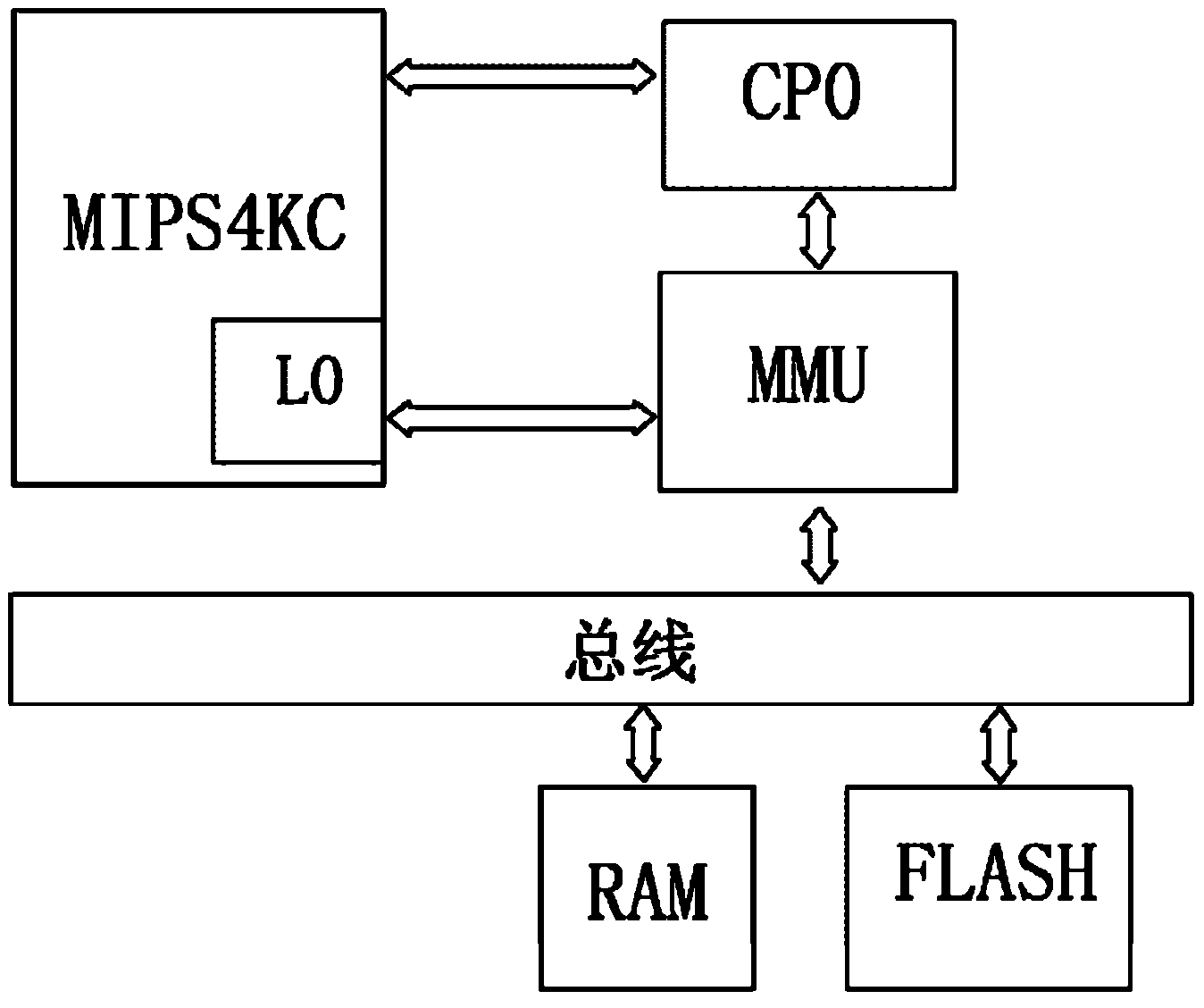
[0029] see figure 1 , a schematic diagram of the composition of an embodiment of the novel instruction cache system of the present invention, taking a SoC chip as an example. The new instruction cache system includes a microprocessor, a system control coprocessor (CP0), and a memory management unit (MMU). In this embodiment, the microprocessor adopts a single-core structure of the MIPS 4Kc system. MIPS 4Kc and CP0, MIPS 4Kc and MMU, and CP0 and MMU respectively establish connections for access control and processing of instructions. Based on the MIPS 4Kc architecture, CP0 can assist the processor to complete operations such as exception / interrupt handling, cache filling, look-aside translation buffer (TLB) decoding filling, and operation mode conversion. MMU is a control line used to manage virtual memory and physical memory. It establishes a connection with memory (RAM) or other external memory (such as: Flash) through a bus. It is also responsible for mapping virtual addres...
Embodiment 2
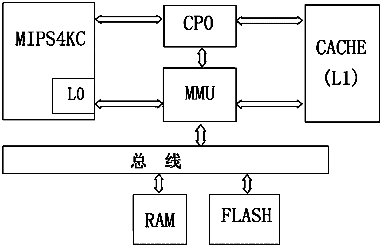
[0035] The structure of the instruction cache system in the second embodiment is roughly the same as that in the first embodiment, so we won’t repeat them here. figure 2 , is a schematic structural diagram of another embodiment of the novel instruction cache system of the present invention. Among them, the CP0 establishes a connection with the L1, and the MMU also establishes a connection with the L1, which can manage the access of instructions stored in the L1. The microprocessor can read instructions stored in L1 or RAM through the MMU. L1 is a traditional four-way set-associative cache with 128 blocks per way, and each block is four words in size. L1 has a tag value, and its Tag has 27 bits, including the high 21-bit physical address bits, 4 effective bits, and 1 replacement bit (using the latest filling algorithm, that is, if a cache line is filled, the replacement of the cache line The bit is 1, and the replacement bit of other cache lines in the row is 0) and 1 lock b...
Embodiment 3
[0050] The composition of the new instruction cache system in the third embodiment of the present invention is substantially the same as that in the second embodiment, except that the microprocessor uses SMP technology such as dual-core or quad-core instead of single-core technology. Since each core has its own instruction fetching module and first-level cache independently, the novel instruction cache system composed of L0 and L1 described in the present invention can also improve the instruction fetching speed of each core and reduce system power consumption, thereby Increase execution speed and accomplish more tasks. For the specific working principles and implementation methods of L0 and L1, reference may be made to Embodiment 1 and Embodiment 2, which will not be repeated here.
PUM
 Abstract
Description
Claims
Application Information
 - R&D
- Intellectual Property
- Life Sciences
- Materials
- Tech Scout
- Unparalleled Data Quality
- Higher Quality Content
- 60% Fewer Hallucinations
Browse by: Latest US Patents, China's latest patents, Technical Efficacy Thesaurus, Application Domain, Technology Topic, Popular Technical Reports.
© 2025 PatSnap. All rights reserved.Legal|Privacy policy|Modern Slavery Act Transparency Statement|Sitemap|About US| Contact US: help@patsnap.com


