
Manufacture method for planar lightwave circuit (PLC) optical device

A manufacturing method and device technology, which is applied in the manufacture of optical waveguides and planar optical splitters, can solve the problems of high raw material requirements, high maintenance costs, and difficult manufacturing, and achieve simple process, lower production costs, Realize the effect of industrial scale production

Inactive Publication Date: 2012-07-04
SUZHOU ORIENTAL SEMICONDUCTOR CO LTD
View PDF3 Cites 2 Cited by
  • Summary
  • Abstract
  • Description
  • Claims
  • Application Information

AI Technical Summary

Problems solved by technology

However, the problem exists in high investment in equipment, high maintenance costs, and high requirements for raw materials (all imported materials are used), and this technology is difficult to manufacture

Method used


Image

  • Manufacture method for planar lightwave circuit (PLC) optical device
  • Manufacture method for planar lightwave circuit (PLC) optical device
  • Manufacture method for planar lightwave circuit (PLC) optical device

Examples


Embodiment Construction

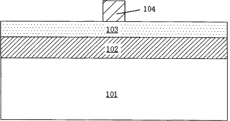
[0025] The present invention will be further described in detail below in conjunction with the accompanying drawings and specific embodiments. In the drawings, for the convenience of illustration, the thicknesses of layers and regions are enlarged or reduced, and the sizes shown do not represent actual sizes. Although these figures do not fully reflect the actual size of the device, they still completely reflect the mutual positions between the regions and the constituent structures, especially the upper-lower and adjacent relationships between the constituent structures. Meanwhile, in the following description, the term substrate used can be understood to include the semiconductor substrate being processed, possibly including other thin film layers prepared thereon.

[0026] Figure 2a It is a schematic diagram of an embodiment of the optical waveguide provided by the present invention, wherein the direction indicated by ab is the propagation direction of light in the optical...


PUM

PropertyMeasurementUnit
Thickness rangeaaaaaaaaaa
Thicknessaaaaaaaaaa
Widthaaaaaaaaaa

Abstract

The invention belongs to the technical field of planar lightwave circuit splitters (PLC splitters), in particular relates to a manufacture method for optical waveguide, and comprises the steps of depositing a layer of photoresist on a glass substrate; performing photoetching to form an image; forming optical waveguide core layers with high reflection rate in a groove between the photoresist; curing the photoresist; and forming a wrapping layer on a membrane with a the high reflection rate. The manufacture method for the optical waveguide is simple in technology process and low in technical difficulty. Requirements for raw materials and production equipment are low, production cost is reduced, and industrialized mass production is easy to achieve.

Description

technical field [0001] The invention relates to a method for manufacturing a planar lightwave circuit (PLC), in particular to a method for manufacturing an optical waveguide, and belongs to the technical field of PLC splitters. Background technique [0002] At present, the construction of FTTX (fiber-optic access network) is gradually unfolding, specifically to realize FTTC (fiber-to-the-curb), FTTB (fiber-to-the-building), FTTH (fiber-to-the-home), FTTD (fiber-to-the-desktop), triple play ( Voice network, data network, cable TV network) and other multimedia transmission and PDS (integrated wiring system) solutions. To build an all-fiber network, in addition to the need for various structural distribution cables and lead-in cables to realize the connection and redistribution of the fiber network, a large number of optical splitters are also required to finally complete the purpose of fiber-to-the-home. [0003] PLC optical devices are generally made on six materials, which ...

Claims


Application Information

Patent Timeline
IPC IPC(8): G02B6/136
Inventor 刘磊刘伟王鹏飞
Owner SUZHOU ORIENTAL SEMICONDUCTOR CO LTD
Learn More