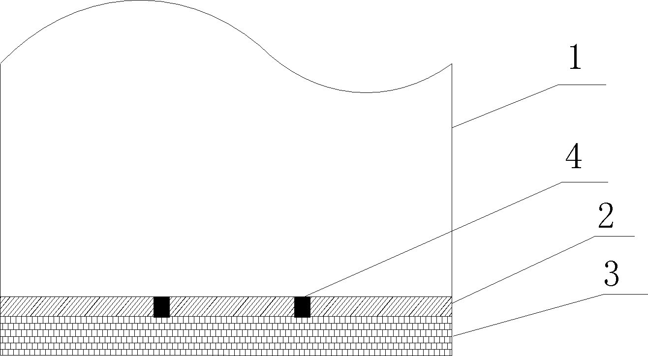
Cell piece possessing back reflection layer and manufacturing method thereof
A technology of back reflective layer and reflective layer, which is applied in the manufacture of circuits, electrical components, final products, etc., can solve the problems of three-dimensional back reflective layer with many raw materials, complicated production process, and increased production cost, so as to facilitate thinning and strengthening The effect of simple absorption and production process
- Summary
- Abstract
- Description
- Claims
- Application Information
AI Technical Summary
Problems solved by technology
Method used
Image
Examples
Embodiment 1
[0021] Embodiment 1 The preparation method of the battery sheet of the present invention
[0022] Take the silicon wafer on which the front anti-reflection film has been prepared, and on the back side, PECVD prepares 90nm thick SiO x Reflective layer; screen-printed aluminum paste, distributed in dots, and the area in contact with the back of the silicon wafer accounts for 10% of the entire back. The front electrode is then printed and sintered to form a localized aluminum back field; then, the surface of the SiOx reflective layer is evaporated. A layer of Al metal layer is plated with a thickness of 1 μm, that is, a battery sheet with a back reflection layer is obtained.
Embodiment 2
[0023] Embodiment 2 The preparation method of the battery sheet of the present invention
[0024] Take the silicon wafer on which the front anti-reflection film has been prepared, and on the back side, PECVD prepares 90nm thick SiO x Reflective layer; screen-printed aluminum paste, distributed in a mesh, and the area in contact with the back of the silicon wafer accounts for 5% of the entire back. Then the front electrode is printed and sintered to form a localized aluminum back field; then, on the SiO x A layer of Al metal layer is vapor-deposited on the surface of the reflective layer, and the thickness is 1 μm, that is, a battery sheet with a back reflective layer is obtained.
Embodiment 3
[0025] Embodiment 3 The preparation method of the battery sheet of the present invention
[0026] Take the silicon wafer on which the front anti-reflection film has been prepared, and on the back side, 85nm thick SiO is prepared by PECVD x Reflective layer; screen-printed aluminum paste, distributed in a mesh shape, the area in contact with the back of the silicon wafer accounts for 6% of the entire back, and then the front electrode is printed and sintered to form a localized aluminum back field; then, on the SiO x A layer of Al metal layer is vapor-deposited on the surface of the reflective layer, and the thickness is 0.7 μm, that is, a battery sheet with a back reflective layer is obtained.
PUM
| Property | Measurement | Unit |
|---|---|---|
| thickness | aaaaa | aaaaa |
| thickness | aaaaa | aaaaa |
| thickness | aaaaa | aaaaa |
Abstract
Description
Claims
Application Information
 - R&D
- Intellectual Property
- Life Sciences
- Materials
- Tech Scout
- Unparalleled Data Quality
- Higher Quality Content
- 60% Fewer Hallucinations
Browse by: Latest US Patents, China's latest patents, Technical Efficacy Thesaurus, Application Domain, Technology Topic, Popular Technical Reports.
© 2025 PatSnap. All rights reserved.Legal|Privacy policy|Modern Slavery Act Transparency Statement|Sitemap|About US| Contact US: help@patsnap.com

