Pinter, method, system and processor for manufacturing printed circuit board

A printed circuit board and processor technology, applied in the direction of conductive pattern formation, etc., can solve the problems of complicated printed circuit board process, poor performance stability of PCB board, and high consumption of manpower and material resources, etc., to achieve simple process and reduce equipment, pollution reduction effect

Active Publication Date: 2012-06-20
HUNAN CREATE SCI & TECH
View PDF5 Cites 15 Cited by
  • Summary
  • Abstract
  • Description
  • Claims
  • Application Information

AI Technical Summary

Problems solved by technology

[0004] The existing production of PCB requires manual (or automatic) coating of ink, and the use of multiple sets of equipment such as screen printing machines, dryers, exposure machines, and developing machines can complete the printing of PCB boards and print PCB circuit boards. The process is complex, the cycle is long, and it consumes more manpower and material resources
At the same time, due to the need to use chemical liquid in the process of negative film production, exposure, development, metal via hole, corrosion, etc., the existing way of printing PCB boards causes serious chemical pollution; and due to the negative film production, Development, exposure, corrosion and other conditions are very demanding, and the performance stability of the PCB board prepared by the existing method is poor

Method used


Image

  • Pinter, method, system and processor for manufacturing printed circuit board
  • Pinter, method, system and processor for manufacturing printed circuit board
  • Pinter, method, system and processor for manufacturing printed circuit board

Examples


Embodiment Construction

[0044] The following will clearly and completely describe the technical solutions in the embodiments of the present invention with reference to the accompanying drawings in the embodiments of the present invention. Obviously, the described embodiments are only some, not all, embodiments of the present invention. Based on the embodiments of the present invention, all other embodiments obtained by persons of ordinary skill in the art without making creative efforts belong to the protection scope of the present invention.

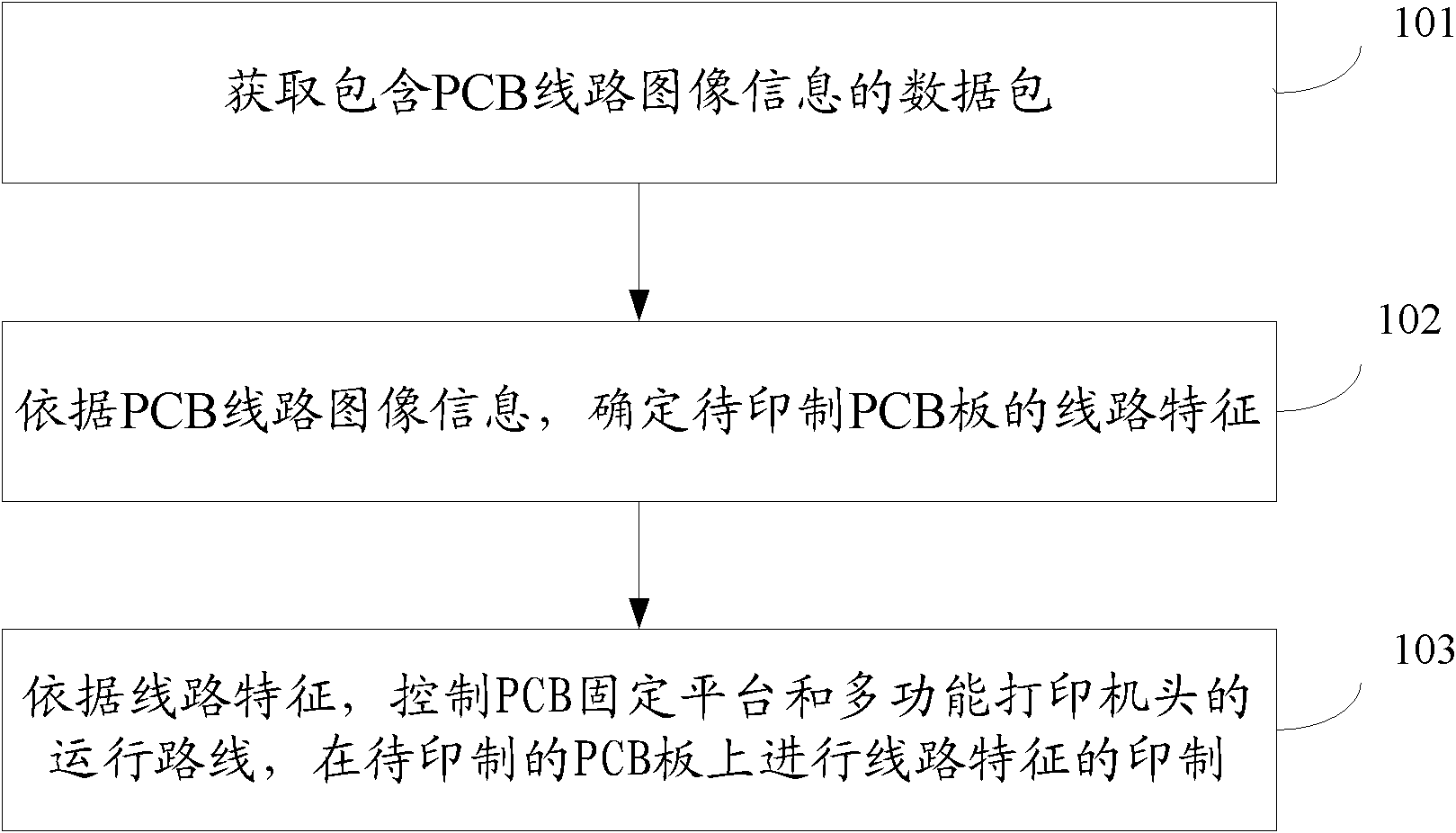
[0045] see figure 1 , shows a schematic flow chart of an embodiment of a method for manufacturing a printed circuit board of the present invention, the method of this embodiment includes:

[0046] Step 101: Obtain a data packet containing PCB circuit image information.

[0047]In general, a computer can be used to design a PCB circuit diagram. In the present invention, the computer processes the circuit diagram designed by the designer or the circuit diagram...


PUM


Abstract

The invention discloses a printer, a method, a system and a processor for manufacturing a printed circuit board (PCB). The method comprises the following steps of: determining relevant characters, such as a line position, a welding pad, a via position, a solder mask position and a character position of the PCB according to the acquired image information of the PCB to be printed; controlling a PCB fixing platform and a multifunctional printer head to operate; and printing the characters, such as a line, a welding pad, a via, a solder mask and a character of the circuit board on the PCB to be printed. According to the method, the PCB can be directly printed without manual coating of ink or exposure and development by using chemical substances, so that the manufacturing process of the PCB is simple and excessive equipment, the consumption of human resources and chemical resources and the pollution are reduced. Meanwhile, the PCB fixing platform and the multifunctional printer head are driven to operate according to the determined line characters, and further the printing position can be accurately controlled; and the printed PCB is higher in precision, so that the manufactured PCB is better in performance.

Description

technical field [0001] The invention relates to the technical field of circuit board production, and more specifically relates to a printer, method, system and processor for producing printed circuit boards. Background technique [0002] In the development and production process of electronic products, it is inevitable to involve the printing of circuit boards. Printed circuit board (PCB, printed circuit board), also known as printed circuit board or printed circuit board, is based on an insulating board, cut to a certain size, on which some lines, pads / vias, solder resist , characters and some conductive graphics to realize the interconnection between electronic components. [0003] At present, in the printing process of PCB board, it is necessary to apply ink on the substrate of insulating material, then dry the ink on the substrate, and then cover the circuit pattern to be made on the substrate coated with ink for exposure. , and finally develop the exposed substrate to...

Claims


Application Information

Patent Timeline
Patent Type & Authority Applications(China)
IPC IPC(8): H05K3/12
Inventor 张宏立李华
Owner HUNAN CREATE SCI & TECH
Why Eureka
Try Eureka