Chip package

A chip and assembly technology, applied in the field of semiconductor assembly, can solve problems such as difficulty in controlling the amount of glue, affecting product reliability, and burdening mold costs, etc.

Inactive Publication Date: 2012-06-20
ADVANCED SEMICON ENG INC
View PDF4 Cites 2 Cited by
  • Summary
  • Abstract
  • Description
  • Claims
  • Application Information

AI Technical Summary

Problems solved by technology

[0004] However, in the past, the encapsulant was mostly formed by molding, so the cost of the mold needs to be borne in the production
Although dispensing or injection can be considered to form the encapsulant, it is not easy to control the amount of glue in this way, and the encapsulant may flow after it is formed on the pre-encapsulated lead frame To the unexpected position, resulting in the problem of glue overflow
[0005] On the other hand, delamination may also occur between the pre-sealed material and the pre-sealed lead frame due to thermal stress or other factors, and the outside air or moisture may be caused by the joint between the pre-sealed material and the pre-sealed lead frame. Access to the inside of the light-emitting diode chip structure, and affect the reliability of the product

Method used


Image

  • Chip package
  • Chip package
  • Chip package

Examples


Embodiment Construction

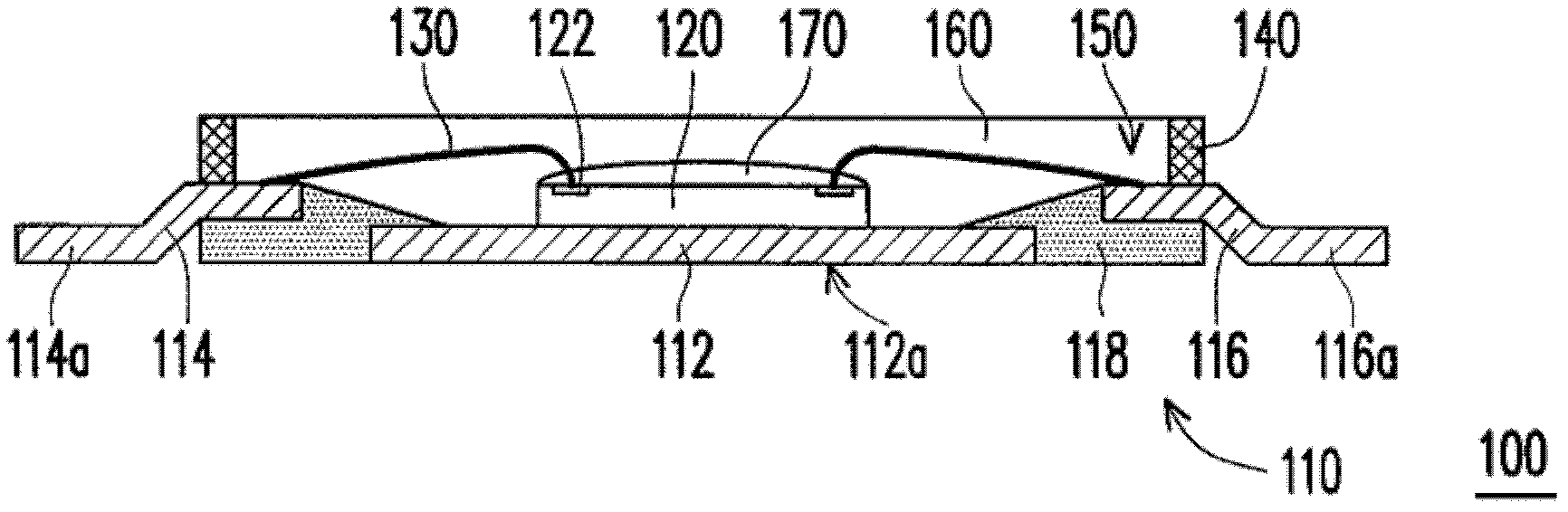
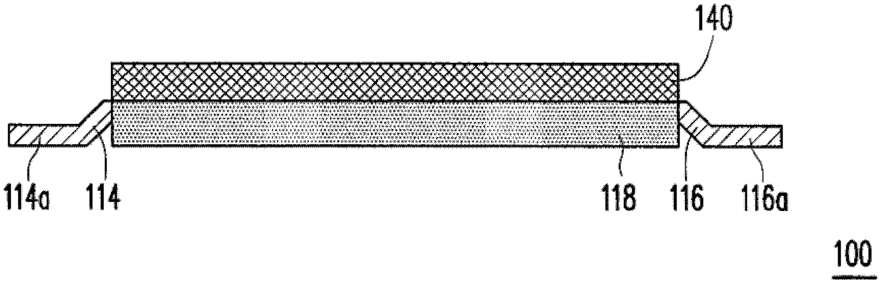
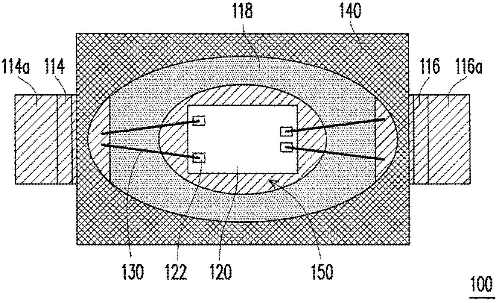
[0066] Please refer to Figure 1A-Figure 1C ,in Figure 1A is a cross-sectional view of a chip structure according to an embodiment of the present invention, Figure 1B and Figure 1C A side view and a top view of the chip assembly, respectively. In order to clearly express the internal structure of the chip structure, Figure 1C Some components are omitted. In this embodiment, the structure of the LED chip 120 is taken as an example to illustrate a technical solution of the present invention, wherein the pre-sealed lead frame 110 is used to carry the LED chip 120, and the pre-sealed lead frame 110 includes a chip holder 112, A plurality of pins (including a positive pin 114 and a negative pin 116 ), and a pre-sealing material 118 . Here, the pre-sealing material 118 is, for example, made of thermoplastic polymer material by injection molding, or thermosetting polymer material by compression molding, especially the thermosetting high polymer material. Molecular materials ...


PUM


Abstract

The invention discloses a chip package, which comprises a pre-molded lead frame, a chip, a plurality of leads, a barricade and a molding compound. A chip carrier and a plurality of pins of the pre-molded lead frame are wrapped by a pre-molding unit in an integrally forming manner, a first portion of each pin extends outside the pre-molding unit, the barricade is disposed on the pre-molded lead frame and connected with the pre-molding unit so as to form a cavity for holding the chip and the leads, the barricade and the pre-molding unit can be made of different materials, and the molding compound is filled into the cavity to cover the chip and the leads.

Description

technical field [0001] The present invention relates to a semiconductor technology, and in particular to a semiconductor assembly technology. Background technique [0002] Semiconductor packaging technology is widely used in various types of electronic component manufacturing processes to connect semiconductor chips to carriers such as substrates or lead frames, or directly bond semiconductor chips to circuit boards to achieve semiconductor chips and external circuits. Connection. [0003] In the conventional LED chip assembly technology, a pre-molded leadframe is used to replace the traditional ceramic substrate to carry the LED chip. The pre-sealed lead frame includes an insulating pre-molding unit, which is used to encapsulate the lead frame with positive and negative leads, wherein part of the positive and negative leads are exposed to the outside of the pre-molding unit . The chip is disposed on a pre-packaged lead frame and coupled to the positive pin and the negati...

Claims


Application Information

Patent Timeline
Patent Type & Authority Applications(China)
IPC IPC(8): H01L33/62H01L33/48
CPCH01L2224/48091H01L2224/48247H01L2224/8592H01L2924/00014
Inventor 詹勋伟
Owner ADVANCED SEMICON ENG INC
Why Eureka
Try Eureka