SnO2 three-dimensional porous photon amorphous semiconductor material and preparation method thereof

An amorphous semiconductor, three-dimensional porous technology, applied in the field of photonic crystals, semiconductor materials and devices, can solve problems such as the inability to prepare only short-term procedures, the difficulty in preparing photonic amorphous crystals, and the inability to prepare photonic amorphous crystals, etc., to achieve Low cost, simple preparation method, effect of reducing requirements

Inactive Publication Date: 2012-06-20
EAST CHINA NORMAL UNIVERSITY
View PDF2 Cites 2 Cited by
  • Summary
  • Abstract
  • Description
  • Claims
  • Application Information

AI Technical Summary

Problems solved by technology

[0004] The self-assembly method can be used to prepare a three-dimensional porous structure, but it can only prepare a periodic structure, and cannot prepare a photonic amorphous with only a short program and a lack of a long program. The phase separation method can also be used to prepare a three-dimensional porous structure. However, It produces holes that are too large to match wavelengths in the visible range
[0005] The present invention solves the problem of SnO in the visible light range of the above-mentioned prior art 2 Due to the difficulties in the preparation of photonic amorphous crystals and the inability to prepare photonic amorphous crystals with only a short program, a method of filling templates by sol-gel method and then removing templates at high temperature to obtain SnO 2 A method for preparing a three-dimensional porous photonic amorphous semiconductor material, which has the beneficial effects of easy acquisition of templates, simple method, low cost, and high repeatability

Method used


Image

  • SnO2 three-dimensional porous photon amorphous semiconductor material and preparation method thereof
  • SnO2 three-dimensional porous photon amorphous semiconductor material and preparation method thereof
  • SnO2 three-dimensional porous photon amorphous semiconductor material and preparation method thereof

Examples


preparation example Construction

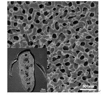
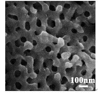
[0024] The present invention uses peach-faced parrot feathers as a template to synthesize SnO 2 A method for preparing a three-dimensional porous photonic amorphous semiconductor material, comprising the steps of:

[0025] Step a, SnCl 2 2H 2 O crystals, absolute ethanol and deionized water are mixed in a molar ratio of 1:100:100-1:150:150 as a source and placed in a beaker, stirred by magnetic force for 2 hours and left to stand for 12 hours to form a precursor; wherein, SnCl 2 2H 2 The purity of O was 99.5%; the purity of absolute ethanol and deionized water were analytically pure.

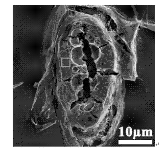
[0026] Step b. Drop 1-5 μL of the precursor onto the edge of the peach-faced parrot feather slice, and then dry the slice at room temperature for about 2 hours.

[0027] Step c. Put the slice in a quartz boat, put it in the middle of a horizontally placed alumina tube furnace, set the heating rate to 1°C / min, raise the temperature to 450-600°C and keep it for 1-2 hours to obtain the product...

Embodiment 1

[0029] The present invention uses peach-faced parrot feathers as a template to synthesize SnO 2 The method for a three-dimensional porous photonic amorphous semiconductor material, the specific steps are as follows:

[0030] 1. Wash and slice parrot feathers on a glass substrate.

[0031] 2. Add SnCl 2 2H 2 O crystals, absolute ethanol, and deionized water were mixed at a molar ratio of 1:100:100 as a source and placed in a beaker to form a cloudy solution.

[0032] 3. Stir the solution for 2 hours by magnetic force and then let it stand overnight for about 12 hours. After that, the solution becomes a transparent single-phase liquid to prepare a precursor solution.

[0033]4. Drop 2 μL of the precursor solution on the edge of the peach-faced parrot feather slice on the glass substrate, and use the capillary effect to penetrate the precursor into the space of the feather, and then dry the slice at room temperature for about 2 hours.

[0034] 5. Put the slice in ...

Embodiment 2

[0039] The present invention uses peach-faced parrot feathers as a template to synthesize SnO 2 The method for a three-dimensional porous photonic amorphous semiconductor material, the specific steps are as follows:

[0040] 1. Wash and slice parrot feathers on a glass substrate.

[0041] 2. Add SnCl 2 2H 2 O crystals, absolute ethanol, and deionized water were mixed at a molar ratio of 1:150:150 as sources and placed in a beaker to form a cloudy solution.

[0042] 3. Stir the solution for 2 hours by magnetic force and then let it stand overnight for about 12 hours. After that, the solution turns into a transparent single-phase liquid to prepare a precursor solution.

[0043] 4. Drop 5 μL of the precursor solution on the edge of the peach-faced parrot feather slice on the glass substrate, and use the capillary effect to penetrate the precursor into the space of the feather, and then dry the slice at room temperature for about 2 hours.

[0044] 5. Put the sl...


PUM


Abstract

The invention discloses a SnO2 three-dimensional porous photon amorphous semiconductor material which comprises a glass substrate and SnO2 three-dimensional porous photon amorphous-structure crystals growing on the surface of the glass substrate. The invention also provides a preparation method of the SnO2 three-dimensional porous photon amorphous semiconductor material, which comprises the following steps: mixing SnCl2.2H2O crystals, anhydrous alcohol and deionized water into a precursor solution; filling a templet, which is a Agapornis roseicollis feather section, by a sol-gel process; and removing the templet at high temperature. The preparation method disclosed by the invention has the advantages of low cost, high repetitiveness and the like; and the prepared SnO2 three-dimensional porous photon amorphous semiconductor material has favorable application prospects in the aspects of photoconducting devices and photon localization research.

Description

Technical field [0001] The invention involves the field of photon crystals, semiconductor materials and device technology, and specifically involves a SNO 2 Three -dimensional multi -pores of non -crystalline non -crystal semiconductor materials and their preparation methods. Background technique [0002] Many bird feathers in nature have natural structural colors. This color comes from the periodic structure inside the feather, not pigment in feathers.For photon crystals composed of periodic structures, they have been widely studied due to their unique light transmission characteristics.And another photon non -crystal material, especially the photon non -crystal that work in the visible light range, also has its unique photogenic transmission phenomenon, such as the localization and random laser of photon.With only short programs and lack of long programs.At present, the methods of preparation of porous structures include self -assembly methods and division methods. None of them...

Claims


Application Information

Patent Timeline
IPC IPC(8): C03C17/23
Inventor 廖娜郁可张正犁朱自强
Owner EAST CHINA NORMAL UNIVERSITY
Why Eureka
Try Eureka