Nanoscale non-volatile resistive random access memory unit and preparation method thereof

A technology of resistive variable memory and memory unit, which is applied in the direction of static memory, digital memory information, information storage, etc. It can solve the problems of large device size, large dispersion of resistive variable performance, and poor stability, and achieve easy integration and easy device performance. control, good performance

Active Publication Date: 2013-11-06
INST OF MICROELECTRONICS CHINESE ACAD OF SCI
View PDF7 Cites 0 Cited by
  • Summary
  • Abstract
  • Description
  • Claims
  • Application Information

AI Technical Summary

Problems solved by technology

[0007] In view of the problems of large device size, large dispersion of resistive performance and poor stability in the existing resistive memory, the purpose of the present invention is to provide a nanoscale non-volatile resistive memory unit using HSG electronic resist

Method used


Image

  • Nanoscale non-volatile resistive random access memory unit and preparation method thereof
  • Nanoscale non-volatile resistive random access memory unit and preparation method thereof
  • Nanoscale non-volatile resistive random access memory unit and preparation method thereof

Examples


Embodiment

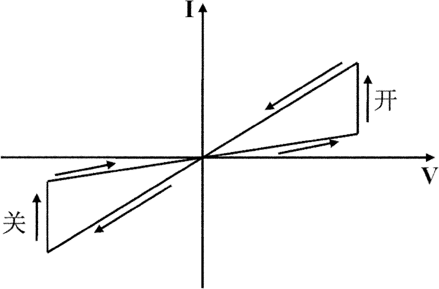
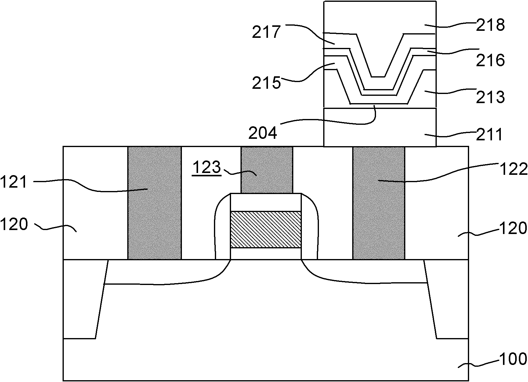
[0105] In one embodiment of the present invention, the plugs 121, 122, and 123 all use tungsten plugs ( Figure 4 ); Magnetron sputtering deposits 20 nanometers thick platinum as the first conductive electrode material 201 ( Figure 5 ); Coating a layer of HSQ negative electron beam resist 202 ( Figure 5 ); using the JEOLJBX-6300FS electron beam lithography system at an accelerating voltage of 100KeV and a beam current of 100pA Figure 6 The pattern shown in the left figure is subjected to electron beam exposure; developing, forming a circular electron beam resist pattern with a diameter of 50 nanometers, i.e. a through hole 203 ( Figure 7 ); Atomic layer deposition of 15 nanometers thick hafnium oxide resistive thin film 205 ( Figure 9 ); Magnetron sputtering deposits 2 nanometers thick copper as the second metal nanolayer film 206 ( Figure 9 ); Atomic layer deposition of 15 nanometers thick hafnium oxide resistive thin film 207 ( Figure 9 ); Magnetron sputtering dep...


PUM

PropertyMeasurementUnit
thicknessaaaaaaaaaa
diameteraaaaaaaaaa
depthaaaaaaaaaa

Abstract

The invention relates to the technical field of semiconductor memories, and discloses a nanoscale non-volatile resistive random access memory unit utilizing a hemi-spherical grain (HSG) electron beam resist and a preparation method thereof. The memory mainly comprises a first conductive electrode, a through-hole, a first resistive material, a second resistive material, a second metal nano layer, a third resistive material and a third conductive electrode, wherein the through-hole and the first resistive material are formed after a hydrogen silsequioxane (HSQ) electron beam resist is exposed and developed via electron beams. A part left after the HSQ electron beam resist is exposed and developed is utilized as the through-hole, the diameter of the through-hole can be as small as a nano magnitude, and the HSQ electron beam resist which is not completely developed at the bottom of the through-hole can be used as a part or the whole of the first resistive material. By utilizing the preparation method, the resistance changing memory which has the advantages of small device area, high yield and good performance can be obtained; and the semiconductor memory is apt to large-scale integration and practicality.

Description

technical field [0001] The invention relates to the technical field of semiconductor memory, in particular to a nanoscale non-volatile resistive variable memory unit using HSG electronic resist and a preparation method thereof. Background technique [0002] The non-volatile memory can keep the stored information for a long time without power on. It not only has the characteristics of ROM, but also has a high access speed. With the demand for large-capacity and low-power storage in multimedia applications and mobile communications, the market share of non-volatile memory, especially flash memory (Flash), is becoming larger and larger, and is also increasing. The more it becomes a very important memory type. Flash memory (Flash) is the mainstream of the non-volatile memory currently on the market, but flash memory devices have excessive operating voltage, slow operating speed, insufficient durability, and excessively thin tunneling oxides in the process of device shrinkage wi...

Claims


Application Information

Patent Timeline
Patent Type & Authority Patents(China)
IPC IPC(8): H01L45/00G11C11/56
Inventor 龙世兵刘明刘琦吕杭炳陈宝钦牛洁斌王艳花张康玮
Owner INST OF MICROELECTRONICS CHINESE ACAD OF SCI
Why Eureka
Try Eureka