Printed circuit board

A technology of printed circuit boards and conductive paths, applied in printed circuits, printed circuit components, circuits, etc., can solve the problems of electrical connectors that cannot meet the requirements and the characteristic impedance becomes smaller, and achieve the effect of improving the characteristic impedance and reducing the capacitance value

Inactive Publication Date: 2012-05-23
FOXCONN (KUNSHAN) COMPUTER CONNECTOR CO LTD +1
View PDF3 Cites 6 Cited by
  • Summary
  • Abstract
  • Description
  • Claims
  • Application Information

AI Technical Summary

Problems solved by technology

A traditional printed circuit board usually includes an insulating substrate, a ground layer, a spacer, and a copper conductive path on the outermost layer. The characteristic impedance of a printed circuit board is usually determined by the width of the conductive path, the thickness of the copper, the dielectric coefficient and thickness of the insulating layer, etc. However, when the conductive path is welded with the external core wire or terminal, the width of the conductive path is often widened due to the large solder joint, resulting in a smaller characteristic impedance, so that the electrical connector using the printed circuit board cannot meet Requirements of the corresponding association

Method used


Image

  • Printed circuit board
  • Printed circuit board
  • Printed circuit board

Examples


Embodiment Construction

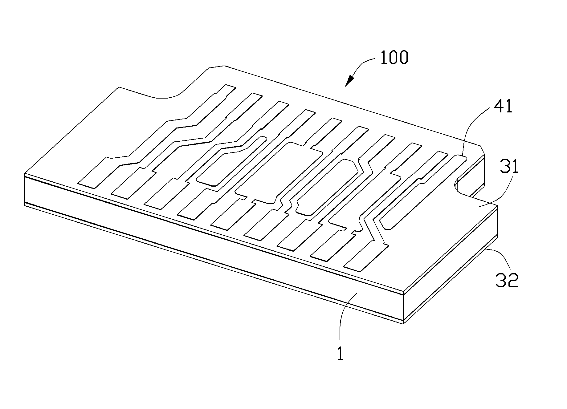
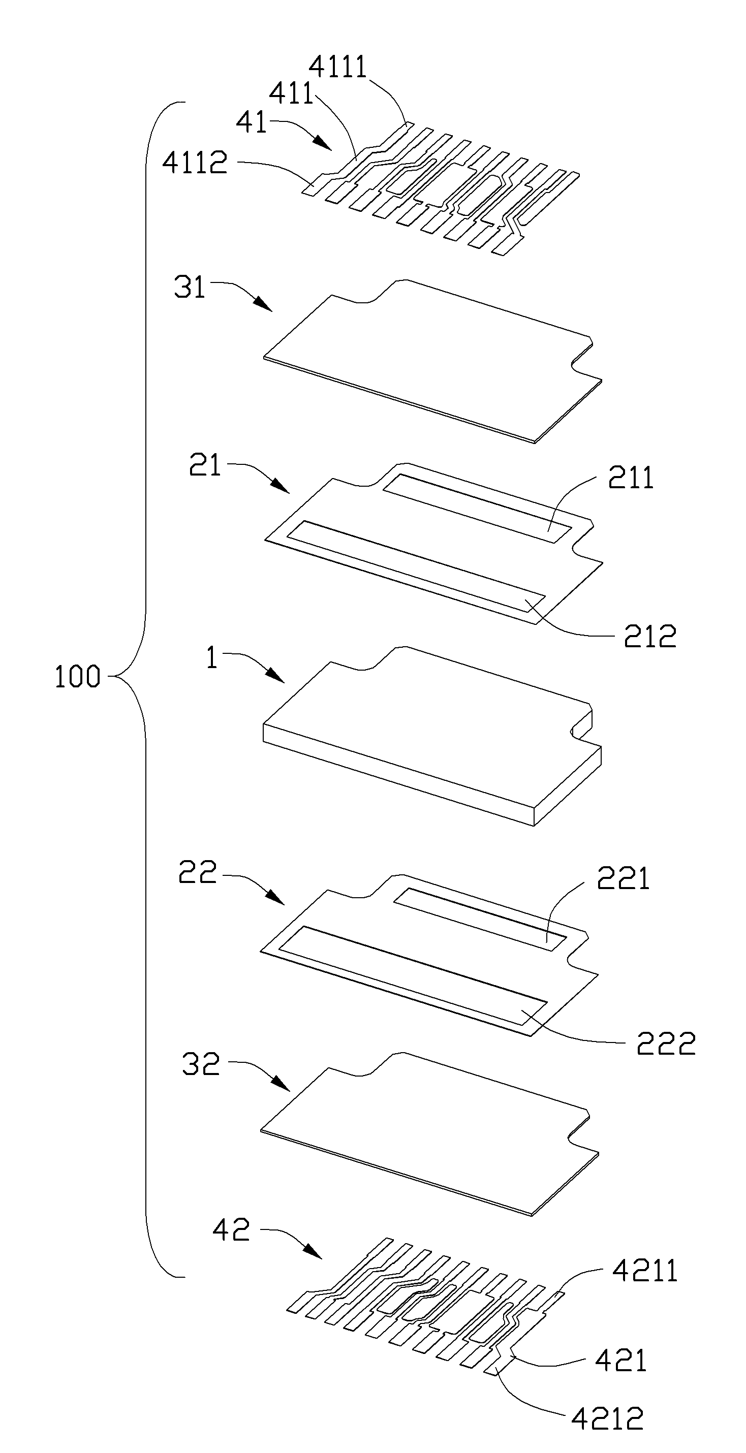
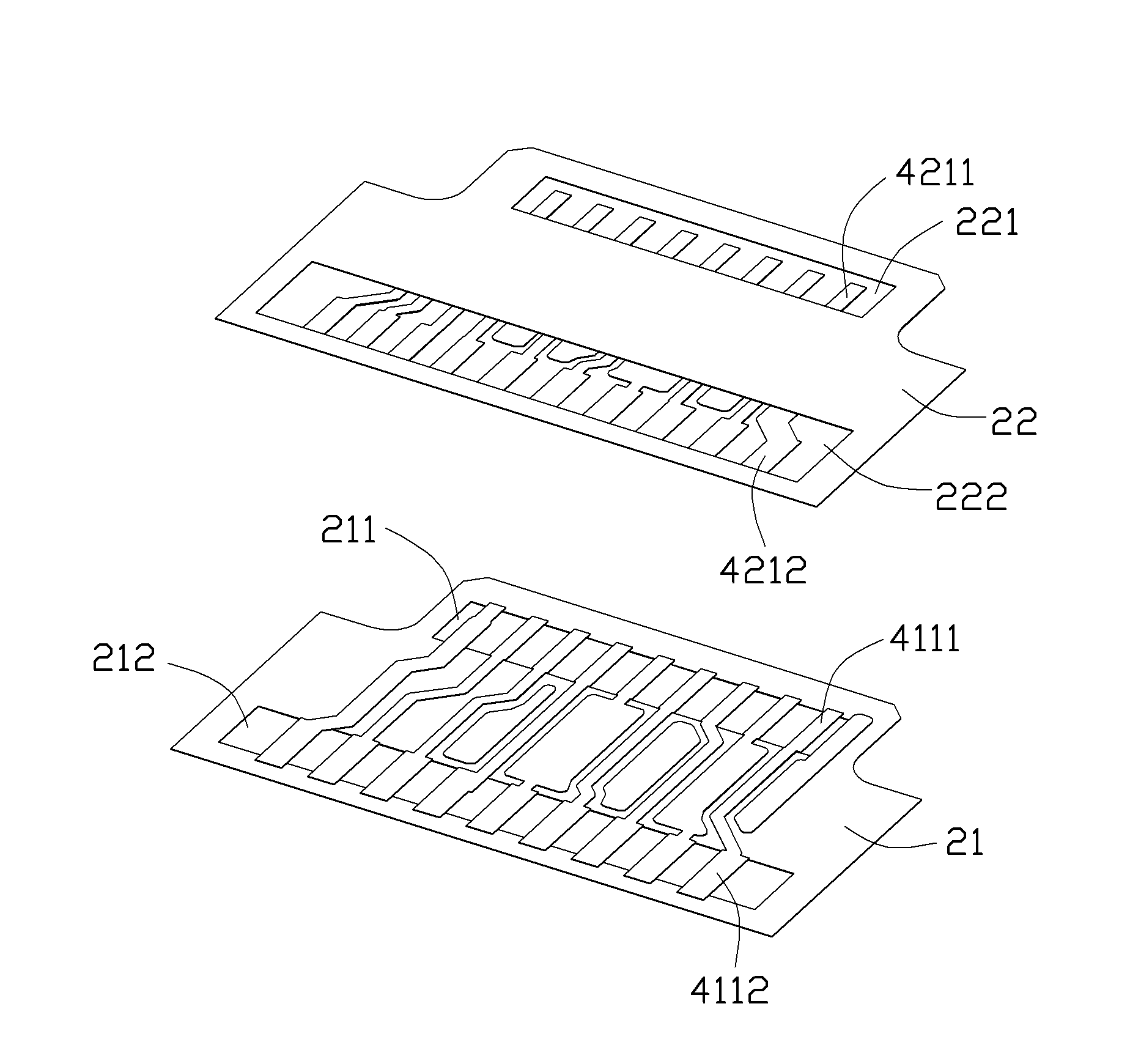
[0010] See Figure 1 to Figure 2 , The printed circuit board 100 of the present invention includes an insulating substrate 1, a first grounding layer 21, a second grounding layer 22, a first interlayer 31, a second interlayer 32, a first conductive path 41, and a second Conductive path 42. The printed circuit board 100 has a convex shape as a whole, but in other embodiments, it may also have other shapes.

[0011] The first ground layer 21 and the second ground layer 22 are printed by copper on the upper and lower surfaces of the insulating substrate 1, respectively. The first ground layer 21 is provided with a first through slot 211 at the front edge and a second through hole at the rear edge. The groove 212 and the second ground layer 22 are provided with a first through groove 221 at the front edge and a second through groove 222 at the rear edge. The first barrier layer 31 is located between the first ground layer 22 and the first conductive path 41, and the second barrier ...


PUM


Abstract

The invention provides a printed circuit board which comprises an insulation substrate, a grounding layer, an interlayer and a conductive path. The insulation substrate, the grounding layer, the interlayer and the conductive path are stacked together along a vertical direction. The conductive path is at an external layer, the interlayer is between the grounding layer and the conductive path. The conductive path comprises a plurality of conducting strips. Each conducting strip comprises at least a weld part. The grounding layer is provided with a channel which is in alignment with the weld part along a vertical direction. A weld part of the conductive path is in vertical alignment with the channel of the grounding layer, thus capacitance values of the conductive path and the grounding layer can be reduced, and characteristic impedance of the printed circuit board is raised.

Description

【Technical Field】 [0001] The invention relates to a printed circuit board, in particular to a printed circuit board inside an electrical connector for transmitting high frequency signals. 【Background technique】 [0002] With the rapid increase in signal transmission speed and the wide application of high-frequency circuits, higher requirements have been placed on printed circuit boards. The circuit performance provided by the printed circuit board must be able to ensure that the signal does not reflect during the transmission process, the signal remains intact, reduces the transmission loss, and plays the role of matching impedance, so as to obtain a complete, reliable, accurate, interference-free, and noise-free transmission signal. Printed circuit boards used in high-frequency electrical connectors are generally bonded together with several layers of materials. A traditional printed circuit board usually includes an insulating substrate, a ground layer, an interlayer, and a c...

Claims


Application Information

Patent Timeline
Patent Type & Authority Applications(China)
IPC IPC(8): H05K1/02H01R13/66
CPCH05K1/117H05K1/0253H05K1/0225
Inventor 苏聘胜陈钧祁锋军王青
Owner FOXCONN (KUNSHAN) COMPUTER CONNECTOR CO LTD
Why Eureka
Try Eureka