Array substrate and method for manufacturing same and liquid crystal display
A technology of an array substrate and a manufacturing method, applied in the field of liquid crystal display, can solve the problems of residual pixel electrode, poor TFT-LCD display, short circuit between the pixel electrode 11 and the common electrode 12, etc., and achieve the effect of improving the yield rate
- Summary
- Abstract
- Description
- Claims
- Application Information
AI Technical Summary
Problems solved by technology
Method used
Image
Examples
Embodiment 1
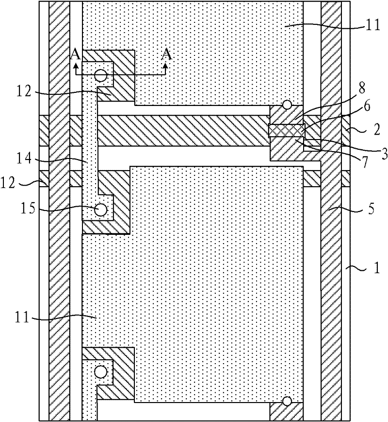
[0050] Figure 2A It is a schematic flow chart of the manufacturing method of the array substrate provided in Embodiment 1 of the present invention, Figure 2B A partial top view structural schematic diagram of an array substrate produced by the method for manufacturing an array substrate provided in Embodiment 1 of the present invention, Figure 2C for Figure 2B The schematic diagram of the side view section structure along the A-A line, such as Figure 2B and Figure 2C As shown, the manufacturing method of the array substrate includes the steps of forming a conductive pattern and an insulating layer on the base substrate 1, the conductive pattern at least includes a gate line 2, a gate electrode 3, an active layer 6, a source electrode 7, and a drain electrode 8. Data lines 5, pixel electrodes 11 and common electrodes 12, wherein one common electrode can correspond to one or more pixel units, and the common electrodes can be connected by common electrode connection line...
Embodiment 2
[0057] Figure 3A It is a schematic flow chart of the manufacturing method of the array substrate provided by Embodiment 2 of the present invention, Figure 3B It is a schematic diagram of a partial top view structure for forming gate lines, gate electrodes, and common electrodes in the method for manufacturing an array substrate provided in Embodiment 2 of the present invention, Figure 3C for Figure 3B The schematic diagram of the side view section structure along the A-A line, such as Figure 3A , Figure 3B and Figure 3C As shown, the blocking block 17 can be arranged on the same layer as the source electrode 7, the drain electrode 8, and the data line 5 and formed synchronously. In this embodiment, taking the insulating layer including the passivation layer 9 and the gate insulating layer 4 as an example, the array The manufacturing method of the substrate specifically includes: firstly, depositing a gate metal layer on the base substrate 1, forming the gate line 2,...
Embodiment 3
[0067] Figure 4A For a schematic flowchart of the method for manufacturing an array substrate provided in Embodiment 3 of the present invention, see Figure 4A , Figure 3B and Figure 3C , the blocking block 17 can be arranged on the same layer as the active layer 6, the source electrode 7, the drain electrode 8, and the data line 5 and formed synchronously. In this embodiment, the insulating layer includes a passivation layer 9 and a gate insulating layer 4 as an example. The manufacturing method of the array substrate specifically includes: firstly, after forming the gate line 2, the gate electrode 3, and the common electrode 12 on the base substrate 1, the blocking block, the active layer, the source electrode, the drain electrode, and the data line The specific steps may include:
[0068] Step 301, on the substrate on which the patterns of the gate line, common electrode, gate electrode and gate insulating layer are formed, sequentially deposit and form the active lay...
PUM
 Abstract
Description
Claims
Application Information
 - R&D
- Intellectual Property
- Life Sciences
- Materials
- Tech Scout
- Unparalleled Data Quality
- Higher Quality Content
- 60% Fewer Hallucinations
Browse by: Latest US Patents, China's latest patents, Technical Efficacy Thesaurus, Application Domain, Technology Topic, Popular Technical Reports.
© 2025 PatSnap. All rights reserved.Legal|Privacy policy|Modern Slavery Act Transparency Statement|Sitemap|About US| Contact US: help@patsnap.com


