Forming method for memory device

A technology for storage devices and storage areas, which is applied in the manufacture of semiconductor/solid-state devices, electrical components, circuits, etc., can solve the problems of decreased isolation effect of active devices, and achieve the effects of avoiding the decrease of isolation effect, avoiding pollution, and avoiding damage

Inactive Publication Date: 2012-05-16
SHANGHAI HUAHONG GRACE SEMICON MFG CORP
View PDF2 Cites 4 Cited by
  • Summary
  • Abstract
  • Description
  • Claims
  • Application Information

AI Technical Summary

Problems solved by technology

[0008] The problem to be solved by the present invention is to provide a method for forming a storage device, improve the stability of the circuit performance in the peripheral area of ​​the storage device, and avoid the problem that the isolation effect between active devices is reduced

Method used


Image

  • Forming method for memory device
  • Forming method for memory device
  • Forming method for memory device

Examples


Embodiment Construction

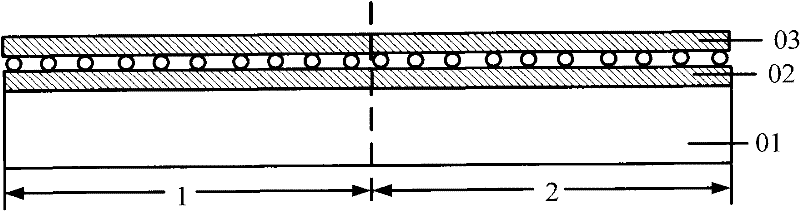
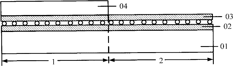
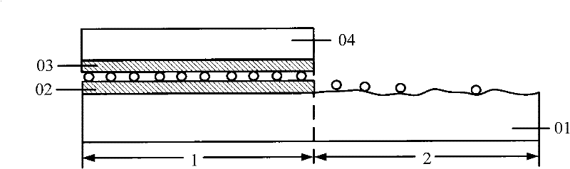
[0029] refer to image 3 , the inventors found that the performance of the circuit in the peripheral region is not stable, and the reasons for the poor isolation effect between the corresponding active devices are as follows: in order to completely remove the nanocrystalline particles, it is necessary to tunnel the tunnels under the nanocrystalline particles Only when the oxide layer 02 is completely removed can the nanocrystalline particles be completely removed, otherwise the nanocrystalline particles will adhere to the tunnel oxide layer 02 and are difficult to remove. At the same time, the thickness of the tunneling oxide layer 02 is small, and its thickness range is approximately 10-30 angstroms, and the tunneling oxide layer 02 is formed by dry thermal growth, with high density and slow removal rate, so it can be completely Removing the tunnel oxide layer 02 under the nanocrystalline particles requires a long removal time, and a long etching time will lead to over-etchin...


PUM

PropertyMeasurementUnit
thicknessaaaaaaaaaa
thicknessaaaaaaaaaa
thicknessaaaaaaaaaa

Abstract

The invention provides a forming method for a memory device. The forming method comprises the following steps of: providing a substrate which comprises a memory area and a peripheral area; forming a sacrificial layer on the substrate of the peripheral area; forming a tunneling oxide layer on the substrate of the memory area; sequentially forming nanocrystalline particles and a top oxide layer on the tunneling oxide layer and the sacrificial layer at the same time; and sequentially removing the top oxide layer, the nanocrystalline particles and the sacrificial layer from the peripheral area, wherein the sacrificial layer is loose, porous and easy to remove at relatively higher etching rate, so that the nanocrystalline particles are completely removed within a relatively shorter etching time without damaging an isolation structure between the substrate and an active device, the stability of performance of a circuit in the peripheral area of the memory device is improved, and the problem that isolation effects among the active devices are worsened is solved.

Description

technical field [0001] The invention relates to the field of semiconductor manufacturing, in particular to a method for forming a memory device. Background technique [0002] Floating gate structure memory devices are currently widely used and generally recognized mainstream memory device types. They are very important semiconductor components and are widely used in the electronics and computer industries. The traditional floating gate structure memory device has the limitations of requiring fast write / erase operations and long-term high-stable storage due to its own structure and material selection, and this contradiction has not been resolved as the technology node shrinks. Significant improvement limits the development of floating gate memory devices. [0003] A memory device with a floating gate structure of nanocrystalline particles, which uses nanocrystalline particles as a charge storage medium, and each nanocrystalline particle is insulated from the surrounding grai...

Claims


Application Information

Patent Timeline
Patent Type & Authority Applications(China)
IPC IPC(8): H01L21/8247H01L21/311
Inventor 曹子贵张雄张博顾靖杨潇楠王永
Owner SHANGHAI HUAHONG GRACE SEMICON MFG CORP
Why Eureka
Try Eureka