Preparation method for pile face black silicon material
A technology of black silicon and suede, applied in the field of solar cells, can solve problems that affect photoelectric conversion efficiency and cannot fully solve the problem of sunlight reflection
- Summary
- Abstract
- Description
- Claims
- Application Information
AI Technical Summary
Problems solved by technology
Method used
Image
Examples
Embodiment 1
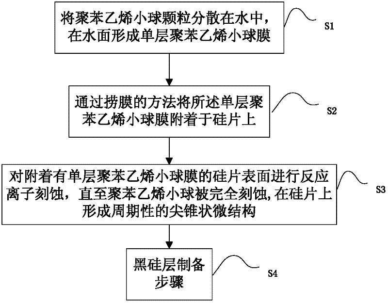
[0030] Preparation method step flow chart of the present invention sees attached figure 1 , a preparation method of suede black silicon material, comprising the following steps:
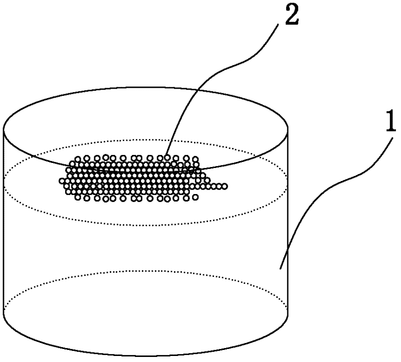
[0031] S1. Disperse polystyrene pellets in water to form a monolayer polystyrene pellet film on the water surface;
[0032] S2. attaching the single-layer polystyrene pellet film to the silicon wafer by the method of pulling film;
[0033] S3. Reactive ion etching is carried out on the surface of the silicon wafer attached with a single-layer polystyrene spherical film, and the gas used in the reactive ion etching is SF 6 , until the polystyrene balls are completely etched, forming a periodic pointed cone-shaped microstructure on the silicon wafer;
[0034] S4. Carrying out the step of preparing a black silicon layer on the silicon wafer prepared in step S3.
[0035] The technological process schematic diagram when the present invention is concretely implemented is referring to appendix figure 2...
Embodiment 2
[0042] Preparation method step flow chart of the present invention sees attached Figure 8 , a preparation method of suede black silicon material, comprising the following steps:
[0043] A1. Disperse the polystyrene bead particles in water to form a single-layer polystyrene bead film on the water surface;
[0044] A2. the single-layer polystyrene bead film is attached to the silicon wafer by the method of pulling film;
[0045] A3. In order to remove a small amount of moisture on the silicon wafer, the silicon wafer attached with a single-layer polystyrene pellet film can be placed in an oven for drying, and the temperature of the oven is controlled at 50-100°C, preferably 60°C in this embodiment;
[0046] A4. Reactive ion etching is performed on the surface of the silicon wafer with a single-layer polystyrene spherical film attached, and the etching gas for reactive ion etching is SF 6 , stop the reactive ion etching when the single-layer polystyrene ball film is not compl...
PUM
 Abstract
Description
Claims
Application Information
 - R&D
- Intellectual Property
- Life Sciences
- Materials
- Tech Scout
- Unparalleled Data Quality
- Higher Quality Content
- 60% Fewer Hallucinations
Browse by: Latest US Patents, China's latest patents, Technical Efficacy Thesaurus, Application Domain, Technology Topic, Popular Technical Reports.
© 2025 PatSnap. All rights reserved.Legal|Privacy policy|Modern Slavery Act Transparency Statement|Sitemap|About US| Contact US: help@patsnap.com


