
Manufacturing method of micro-structure optical plate with high transferring rate

A manufacturing method and microstructure technology, applied to optical components, household appliances, and other household appliances, can solve problems such as insufficient transfer rate, unsuitable optical plates, and affecting optical properties

Inactive Publication Date: 2014-02-26
CHI MEI CORP
View PDF7 Cites 0 Cited by
  • Summary
  • Abstract
  • Description
  • Claims
  • Application Information

AI Technical Summary

Problems solved by technology

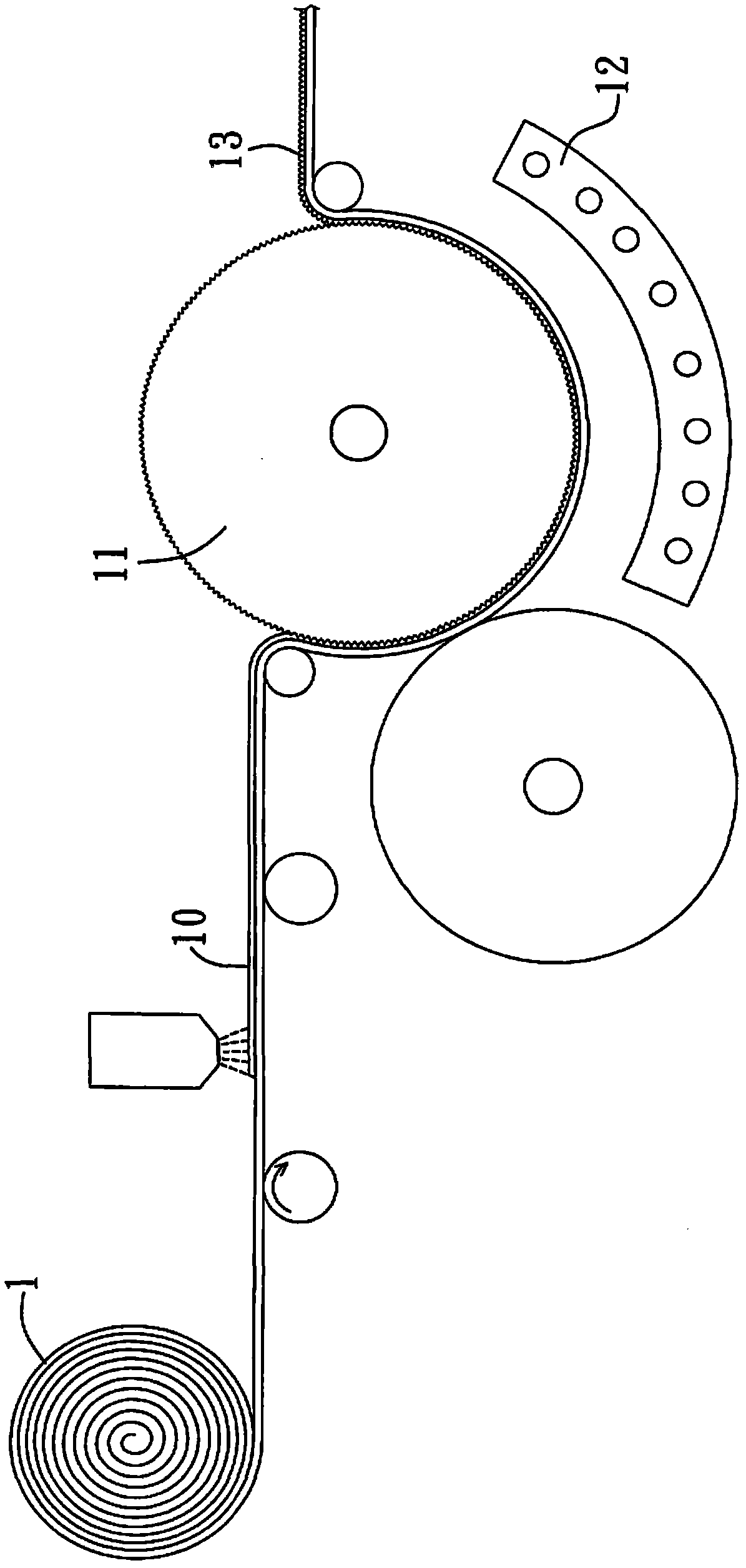
[0003] However, if the optical plate in the back light module of a general liquid crystal display (Liquid Crystal Display), such as a light diffusion plate or a light guide plate, if microstructures are to be formed on the surface, the optical plate cannot be bent directly Fully cover the wheel surface of the transfer roller 11 in a curved form. Therefore, the surface microstructure shape of the transferred optical plate is different from the required surface microstructure shape of the optical plate, which affects the optical properties. The transfer ratio (Transfer Ratio) is insufficient, so the technology for manufacturing the surface microstructure of the optical film shown in the aforementioned Japanese Patent Application No. 2001-113538 is not suitable for making an optical plate with a surface microstructure

Method used

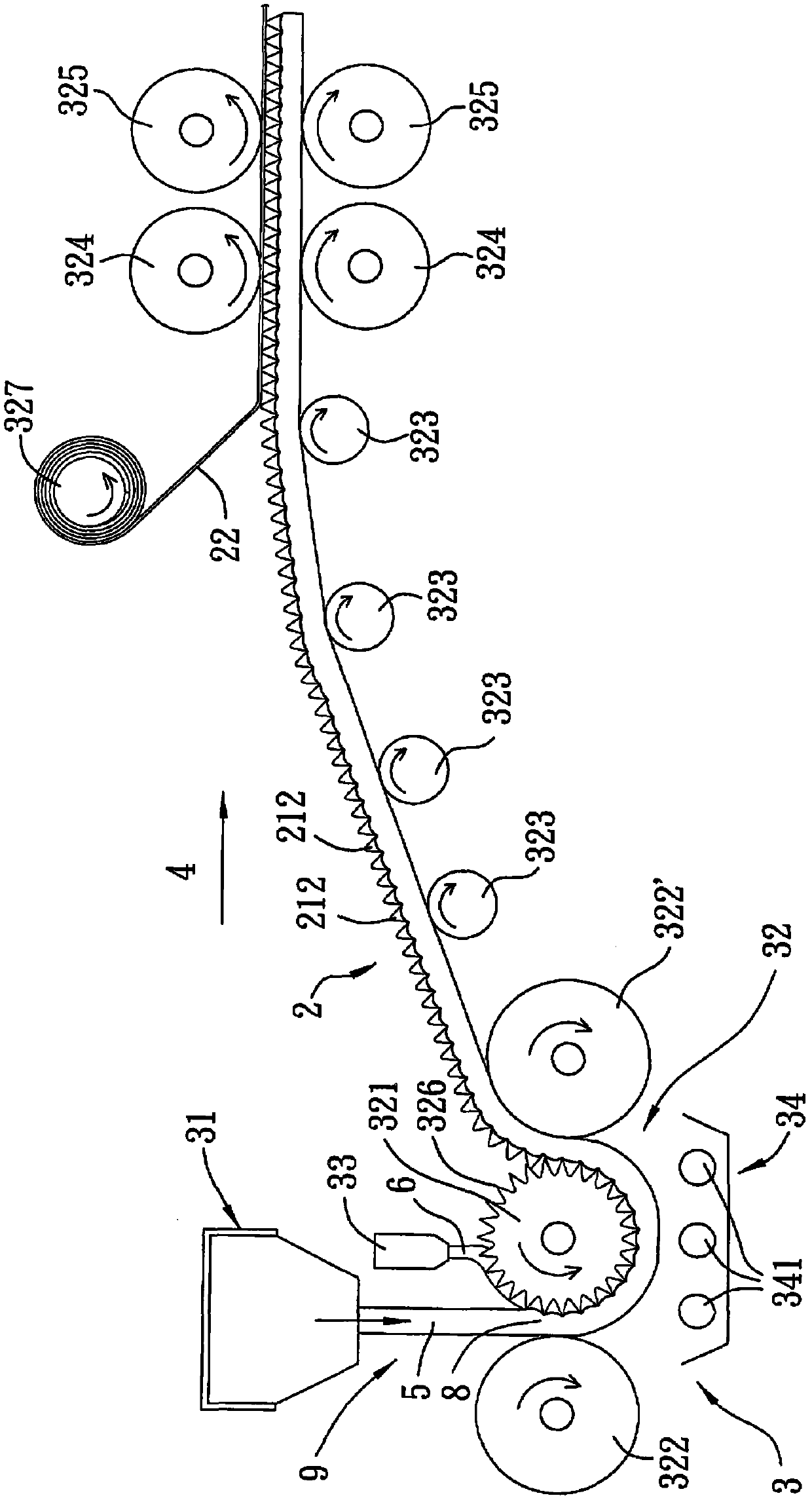

Image

  • Manufacturing method of micro-structure optical plate with high transferring rate
  • Manufacturing method of micro-structure optical plate with high transferring rate
  • Manufacturing method of micro-structure optical plate with high transferring rate

Examples


Embodiment Construction

[0048] Below in conjunction with accompanying drawing and embodiment the present invention is described in detail:

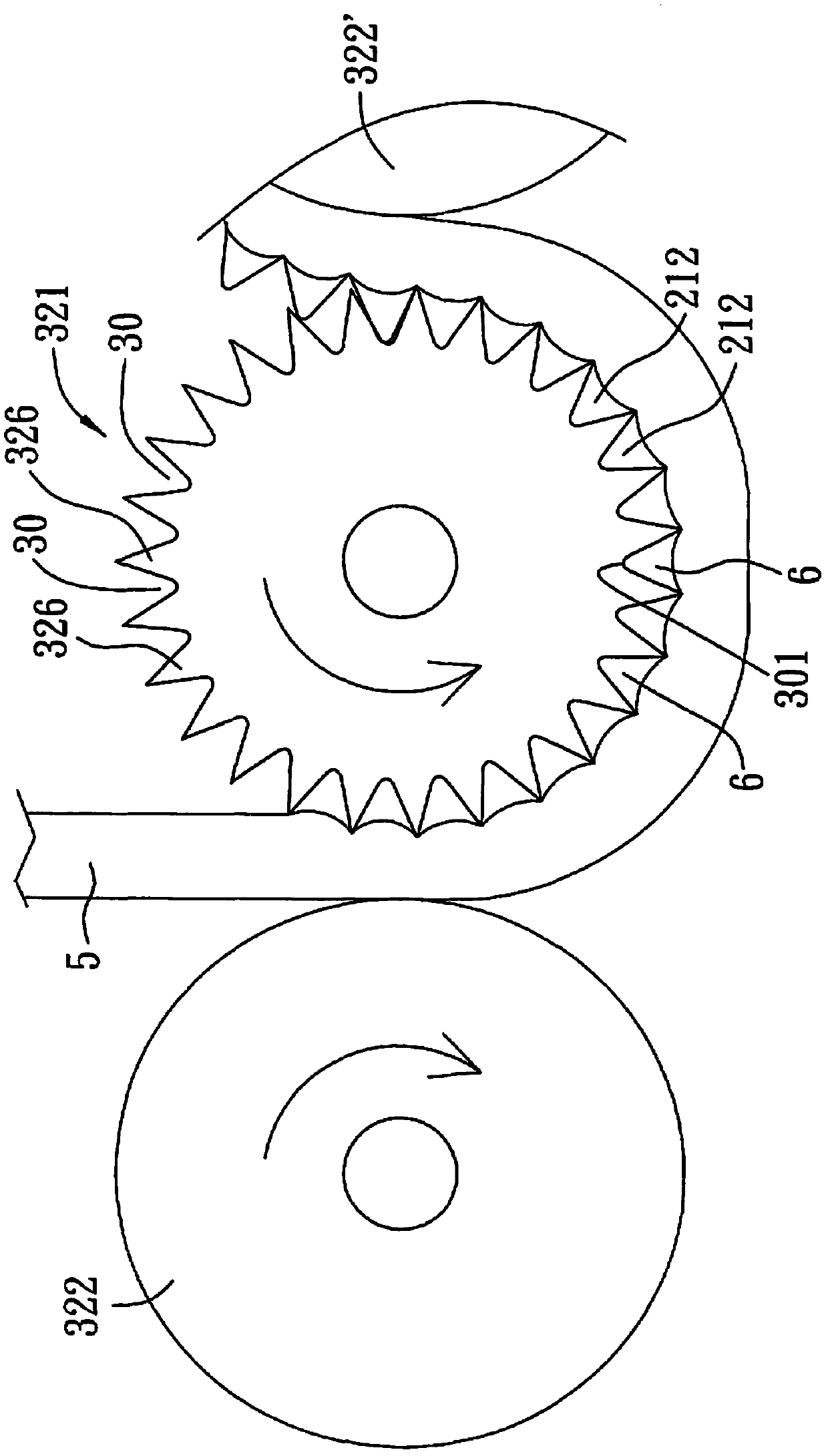
[0049] refer to figure 2 , 3 , 4. A preferred embodiment of the manufacturing method of the present invention is to manufacture a piece of microstructured optical plate 2 through a molding device 3. In this embodiment, the microstructured optical plate 2 is a light diffusion plate, and the molding device 3 includes: a die head 31, a roller unit 32, a photosensitive resin material filling bottle 33, and a set of lighting equipment 34. Wherein, the roller unit 32 includes a transfer roller 321, two pressing rollers 322, 322', multiple adjacent conveying rollers 323, multiple film sticking rollers 324, multiple pulling rollers 325, and a Between the conveying roller 323 at the end and the film sticking roller 324 is a rolling roller 327 for a piece of protective film 22 to be wound. Here define a production line from upstream to downstream for direction 4, in ...


PUM

PropertyMeasurementUnit
thicknessaaaaaaaaaa
glass transition temperatureaaaaaaaaaa

Abstract

The invention relates to a manufacturing method of a micro-structure optical plate with a high transferring rate. According to the method, a high-temperature resin material is extruded from a mold head, and is injected into a space between a pressing roller and a transferring roller; a photosensitive resin material which can be hardened with illumination is then injected, such that the photosensitive resin material flows between the surface of the resin material and the surface of the transferring roller; illumination is provided; the temperature of the material extruded from the mold head and the temperature of the resin material contacting the transferring roller are appropriately adjusted, such that a relatively high temperature and flexibility of the resin material are maintained, and the resin material is curvedly covered on the surface of the transferring roller; and with the cooperation of the high-fluidity photosensitive resin which is hardened with illumination, the micro-structure optical plate with a high micro-structure transferring rate is obtained.

Description

technical field [0001] The present invention relates to a method for manufacturing a microstructured optical plate, in particular to a method for manufacturing such as a diffuser plate, a light guide plate or other optical plates with different optical effects, and the obtained optical plate has a high microstructure transfer rate Production method. Background technique [0002] In Japanese Laid-Open Patent Application No. 2001-113538, figure 1 It shows a technology for forming microstructures on optical films, which pulls out a piece of optical film substrate 1 that is wound into a roll, and coats a layer of ultraviolet curable resin 10 on the surface of the substrate 1, Then, it is embossed by a transfer roller 11 with a microstructure pattern on the surface, and at the same time, it is illuminated by a group of lighting equipment 12, and the subsequent calendering film step (not shown) is added to form a multi-layer surface with a protruding microstructure 13. layer of ...

Claims


Application Information

Patent Timeline
Patent Type & Authority Patents(China)
IPC IPC(8): B29C43/28B29C43/58B29L11/00
Inventor 陈信宏曾炜展王崇豪
Owner CHI MEI CORP
Learn More