


Quick Research
Generate reliable direction feasibility study reports for your R&D in just a few steps.

Technical Q&A
Discover and master advanced knowledge NOW. Basics, ideas, possibilities, all at once.

Find Solutions
As an expert in R&D theories, this can generate solutions to your technical problems instantly.

Evaluate Feasibility
Analyze your overall solution with one click, know your potential R&D risks in advance.

Monitor Landscape
Get weekly tech updates, stay abreast of the latest tech innovations and key insights.
Light-emitting diode with region protection layer
A technology for light-emitting diodes and area protection, which is applied to semiconductor devices, electrical components, circuits, etc., and can solve problems such as increased solder joint drop-off, light interference, and drop
- Summary
- Abstract
- Description
- Claims
- Application Information
AI Technical Summary
Problems solved by technology
Method used
Image

Examples
Embodiment Construction
[0048] The following description and examples are used to explain the details of the present invention. However, those skilled in the art should easily understand that under the coverage of the embodiments of the present invention, there should be considerable changes and improvements to the above-mentioned embodiments. Therefore, the following embodiments are not intended to limit the protection scope of the present invention.
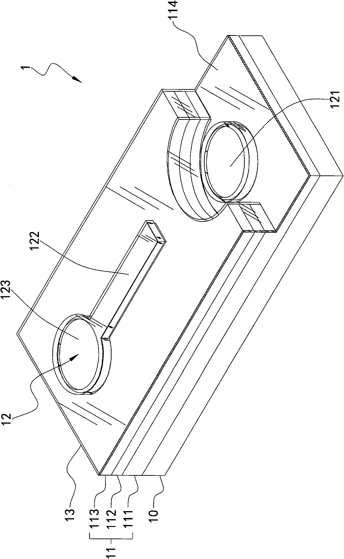
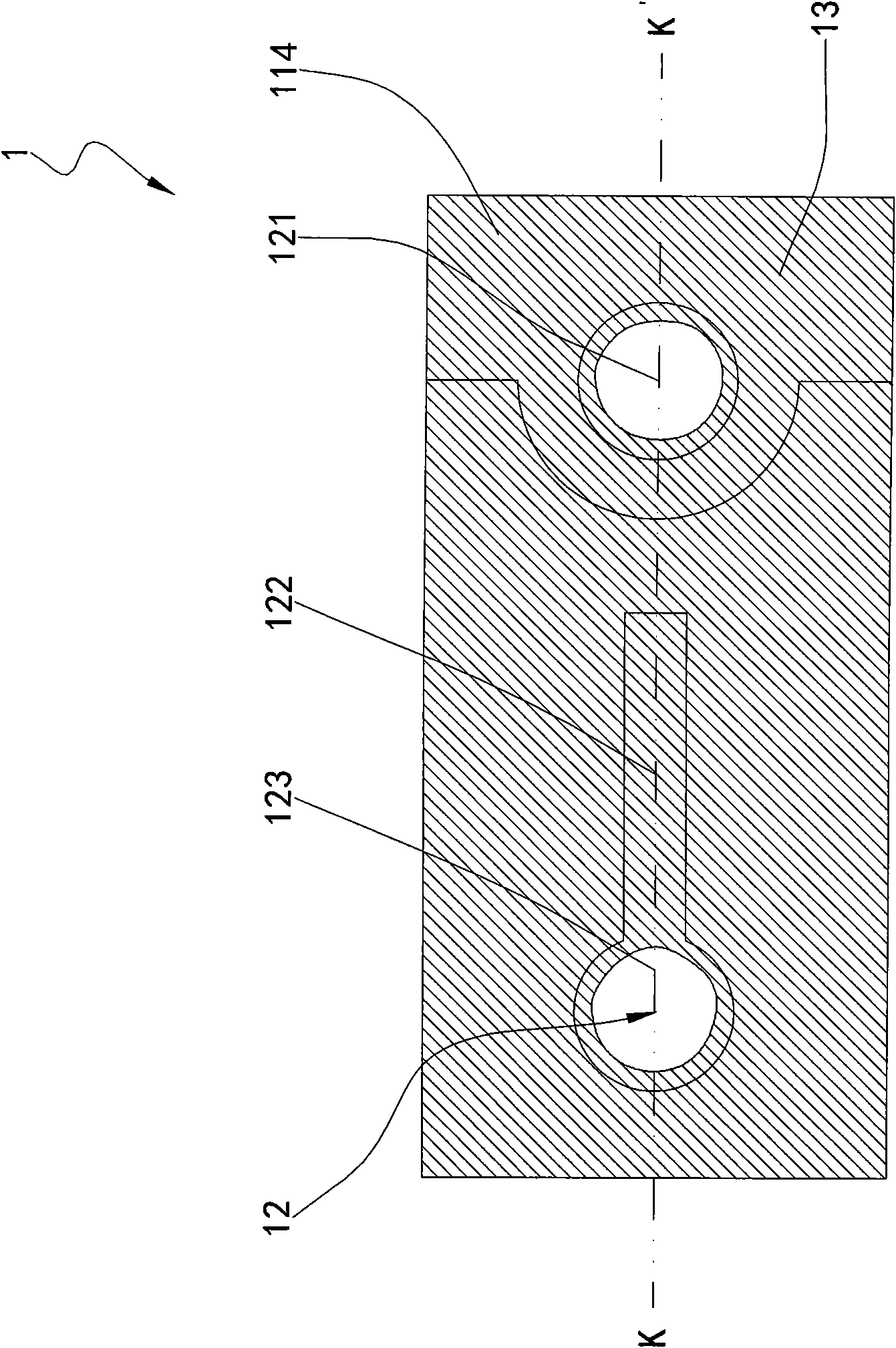
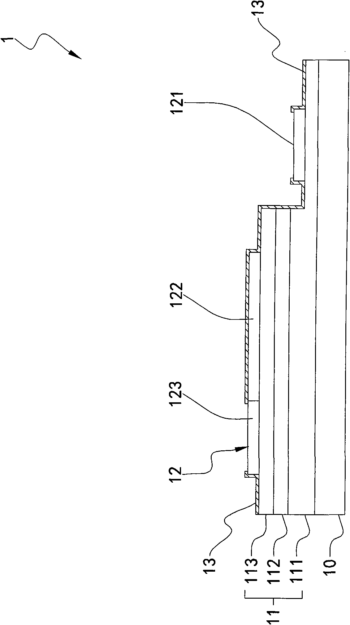
[0049] See Figure 2A As shown, it shows a three-dimensional structure diagram of a light emitting diode 2 with a region protection layer according to the first embodiment of the present invention, which includes a substrate 20 , a light emitting stack 21 and an electrode group 22 . Wherein, the light-emitting laminated layer 21 is grown on the substrate 20 by semiconductor technology and epitaxy technology, and the semiconductor technology may include deposition (deposition) technology, yellow light (photo) technology, etching (etching) technology, ...
PUM
 Abstract
Description
Claims
Application Information
 - R&D Engineer
- R&D Manager
- IP Professional
- Industry Leading Data Capabilities
- Powerful AI technology
- Patent DNA Extraction
Browse by: Latest US Patents, China's latest patents, Technical Efficacy Thesaurus, Application Domain, Technology Topic, Popular Technical Reports.
© 2024 PatSnap. All rights reserved.Legal|Privacy policy|Modern Slavery Act Transparency Statement|Sitemap|About US| Contact US: help@patsnap.com