PCB (printed circuit board) and base station communication equipment

A PCB board and board technology, applied in the field of electronic equipment, can solve the problems of low product integration, high production cost, and large product volume, and achieve the effects of high product integration, reduced production costs, and reduced intermodulation interference

Active Publication Date: 2013-09-11
HUAWEI TECH CO LTD
View PDF6 Cites 0 Cited by
  • Summary
  • Abstract
  • Description
  • Claims
  • Application Information

AI Technical Summary

Problems solved by technology

[0002] At present, PCB boards that can meet the requirements of low intermodulation are usually composed of a single material, and the price of this single material is usually very high, and the cost of making a multi-layer PCB board is very high
Moreover, due to the high production cost, only the modules with low intermodulation requirements are placed on the high-cost low intermodulation PCB board, and other modules without low intermodulation requirements are placed on another common PCB board, and the product integration is low.
Then, the low-intermodulation PCB board is connected to the ordinary motherboard through a coaxial cable with a high price, and the diameter of the coaxial cable is relatively large, which is not easy to bend, which is not conducive to the portability of the product, and the product is large in size and high in cost.

Method used


Image

  • PCB (printed circuit board) and base station communication equipment
  • PCB (printed circuit board) and base station communication equipment
  • PCB (printed circuit board) and base station communication equipment

Examples


Embodiment 1

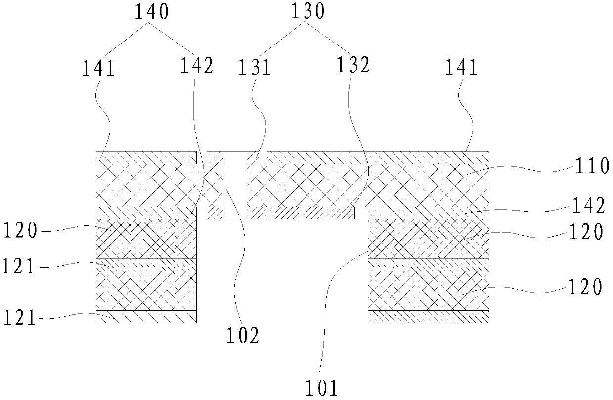
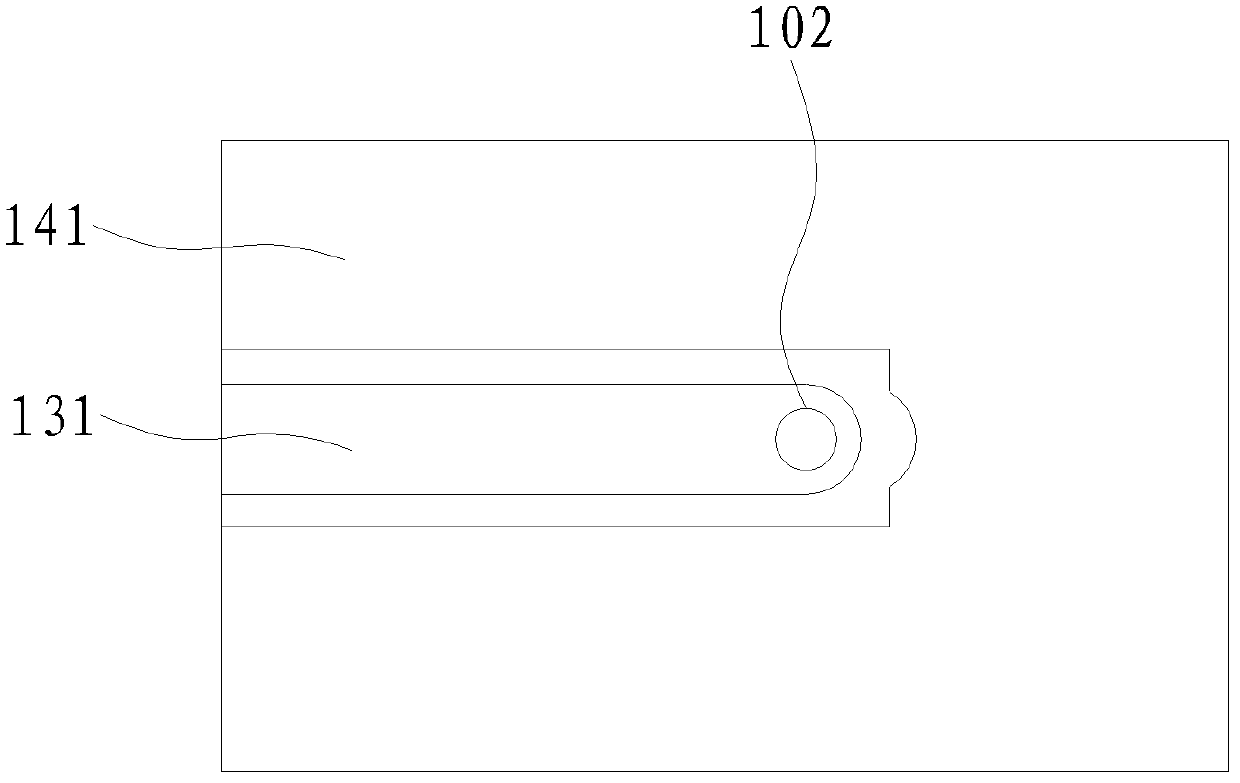
[0022] Specifically, such as figure 1 and image 3As shown, the ordinary sheet material layer 120 is attached on the other side of the low intermodulation sheet material layer 110 , and the avoidance groove 101 is correspondingly opened at the area of ​​the inner signal copper foil layer 132 . In this embodiment, the common board layer 120 is stacked on the same side of the low intermodulation board layer 110 . The escaping groove 101 can be set on one or two or more common sheet layers 120 closest to the low intermodulation sheet layer 110 , the details can be determined according to the actual situation, and all belong to the protection scope of the present invention. The inner signal copper foil layer 132 is exposed in the air, so as to avoid the intermodulation interference caused by the common board layer 120 .

Embodiment 2

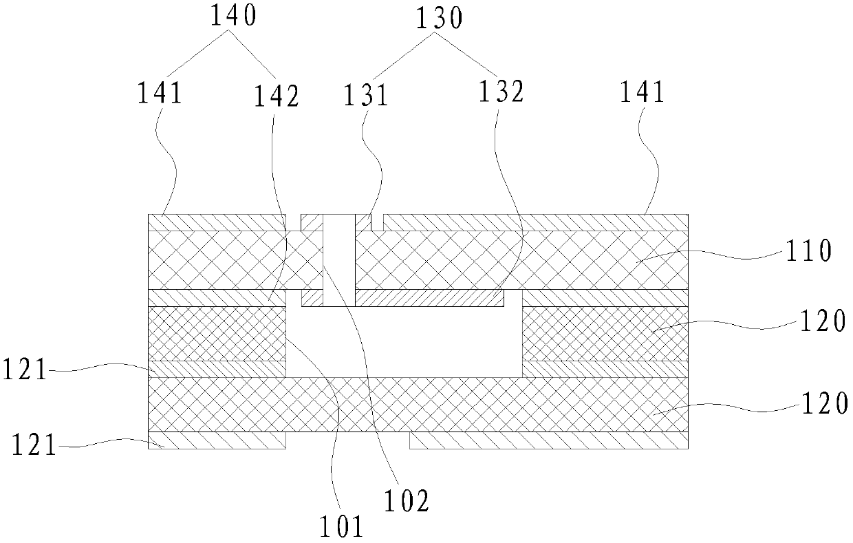
[0024] or, as in Figure 4 As shown, the common board layer 120 is respectively arranged on one side and the other side of the low intermodulation board layer 110, and the avoidance groove 101 is opened on one side and the other side of the low intermodulation board layer 110 respectively. on the common board layer 120 on the side, and correspond to the surface signal copper foil layer 131 and the inner signal copper foil layer 132 respectively. The escaping groove 101 can be set on one or two or more common sheet layers 120 closest to the low intermodulation sheet layer 110 , the details can be determined according to the actual situation, and all belong to the protection scope of the present invention.

Embodiment 3

[0026] or, if Figure 5 As shown, the common plate layer 120 and the low intermodulation plate layer 110 are both provided with at least two layers, and the common plate layer 120 and the low intermodulation plate layer 110 are alternately stacked. The empty slot 101 is matched with the surface signal copper foil layer 131 or / and the inner signal copper foil layer 132 , which satisfies the requirement of low intermodulation while meeting the wiring requirement of the PCB.


PUM


Abstract

The invention is applicable to electronic equipment techniques and discloses a PCB (printed circuit board) and base station communication equipment. The PCB comprises at least one low intermodulation plate layer and at least one common plate layer which are laminated, wherein the low intermodulation plate layer is provided with a signal conducting area and a non signal conducting area; the common plate layer adjacent to the low intermodulation plate layer is provided with an avoidance groove which enables the signal conducting area to be exposed in air; and the avoidance groove is correspondingly arranged at the signal conducting area adjacent to the common plate layer. The base station communication equipment comprises the PCB. The PCB and the base station communication equipment, which are provided by the invention, can meet a low intermodulation requirement and further have low production cost; and the integrated level of products can be improved, and the portability of the product can be facilitated, and the product has a small volume.

Description

technical field [0001] The invention belongs to the technical field of electronic equipment, and in particular relates to a PCB board and base station communication equipment. Background technique [0002] At present, PCB boards that can meet the requirements of low intermodulation are usually composed of a single material, and the price of this single material is usually very high, and the cost of making a multi-layer PCB board is very high. Moreover, due to the high production cost, only the modules with low intermodulation requirements are placed on the high-cost low intermodulation PCB board, and other modules without low intermodulation requirements are placed on another common PCB board, and the product integration is low. . Then, the low-intermodulation PCB board and the ordinary motherboard are connected by a relatively expensive coaxial cable, and the diameter of the coaxial cable is relatively large, which is not easy to bend, which is not conducive to the portabi...

Claims


Application Information

Patent Timeline
Patent Type & Authority Patents(China)
IPC IPC(8): H05K1/02H04W88/08
Inventor 陈海广李洪彩
Owner HUAWEI TECH CO LTD
Why Eureka
Try Eureka