Liquid crystal display panel and its voltage control method

A liquid crystal display panel, voltage technology, applied in static indicators, instruments, etc., can solve the problems of positive and negative voltage asymmetry, image crosstalk, etc., to reduce image jitter and improve display quality.

Active Publication Date: 2014-10-29
TCL CHINA STAR OPTOELECTRONICS TECH CO LTD
View PDF1 Cites 0 Cited by
  • Summary
  • Abstract
  • Description
  • Claims
  • Application Information

AI Technical Summary

Problems solved by technology

[0008] An object of the present invention is to provide a liquid crystal display panel to solve the technical problem of image crosstalk caused by the asymmetry of positive and negative electrode voltages due to the voltage jump of the pixel electrode when the gate voltage of the thin film transistor is turned off.

Method used


Image

  • Liquid crystal display panel and its voltage control method
  • Liquid crystal display panel and its voltage control method
  • Liquid crystal display panel and its voltage control method

Examples


Embodiment Construction

[0059] The following descriptions of the various embodiments refer to the accompanying drawings to illustrate specific embodiments in which the present invention can be practiced.

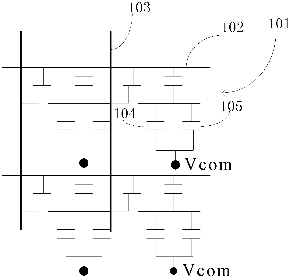
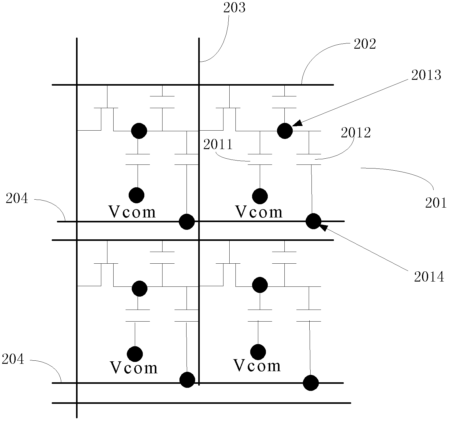
[0060] image 3 It is a circuit structure diagram of a preferred embodiment of the liquid crystal display panel in the present invention.

[0061] The liquid crystal display panel provided by the present invention includes a gate driver, a source driver (not shown in the figure), and also includes a plurality of gate lines 202 and data lines 203, and the plurality of gate lines 202 and the plurality of data lines 203 define multiple Each pixel unit 201 includes a pixel capacitor 2011 , a storage capacitor 2012 , a pixel electrode 2013 and a common electrode 2014 .

[0062] The liquid crystal display panel provided by the present invention further includes thin film transistors (not shown). A thin film transistor includes a gate, a source, and a drain.

[0063] The liquid crystal display panel pr...


PUM


Abstract

A liquid crystal display panel comprises a gate drive, a source drive, multiple gate lines (202) and multiple data lines (203). The multiple gate lines (202) and the multiple data lines (203) define multiple pixel units (201). Each pixel unit (201) comprises a thin film transistor, a common electrode (2012) and a pixel electrode (2013). The data line (203) is used for charging the pixel electrode (2012). The liquid crystal display panel further comprises a common electrode line (204). The common electrode line (204) is connected to the common electrode (2014), and is used for providing an alternating common electrode voltage to the common electrode (2014), so that when a gate voltage of the thin film transistor is turned off, a voltage value of the pixel electrode (2013) is still close to a target voltage value of the pixel electrode (2013) when being charged by the data line (203). Also provided is a voltage control method of a liquid crystal display panel.

Description

【Technical field】 [0001] The invention relates to the technical field of liquid crystal display, in particular to a liquid crystal display panel and a voltage control method thereof. 【Background technique】 [0002] With the continuous development of liquid crystal display technology, users have higher and higher requirements on the quality of liquid crystal display. [0003] see figure 1 , figure 1 It is a driving circuit diagram of a liquid crystal display (Liquid Crystal Display, LCD) panel in the prior art, including a pixel electrode 101 , a gate line 102 , a data line 103 , a pixel capacitor 104 and a storage capacitor 105 . [0004] After the gate voltage (not shown) of the thin film transistor (Thin Film Transistor, TFT) is turned on, an electrical signal is written into the pixel electrode 101 by the data line 103 , giving the pixel electrode 101 a voltage signal to be filled. Afterwards, the gate voltage of the thin film transistor is turned off, and the pixel el...

Claims


Application Information

Patent Timeline
Patent Type & Authority Patents(China)
IPC IPC(8): G02F1/133G09G3/36
CPCG09G3/3655G09G3/3648
Inventor 康志聪
Owner TCL CHINA STAR OPTOELECTRONICS TECH CO LTD
Why Eureka
Try Eureka