
Method of manufacturing multi-layered printed circuit board

A manufacturing method and multi-layer printing technology, applied in multi-layer circuit manufacturing, printed circuit manufacturing, printed circuit, etc., can solve problems such as inability to obtain multi-layer printed wiring boards, difficulty in forming outer layer circuit patterns, etc., and achieve easy electrodeposition Improved performance, reduced plating thickness, finer circuit patterns

Active Publication Date: 2013-05-01
NIPPON MEKTRON LTD
View PDF7 Cites 0 Cited by
  • Summary
  • Abstract
  • Description
  • Claims
  • Application Information

AI Technical Summary

Problems solved by technology

[0032] In order to solve the above-mentioned problem that a multilayer printed wiring board capable of high-density mounting cannot be obtained because it is difficult to form a fine outer layer circuit pattern, the present invention aims to provide a build-up layer having a multilayer hole structure capable of high-density mounting Method for manufacturing multilayer printed wiring board

Method used


Image

  • Method of manufacturing multi-layered printed circuit board
  • Method of manufacturing multi-layered printed circuit board
  • Method of manufacturing multi-layered printed circuit board

Examples


Embodiment Construction

[0057] Hereinafter, the manufacturing method of the build-up type multilayer printed wiring board which has a multilayer via structure concerning embodiment of this invention is demonstrated, referring drawings.

[0058] In addition, the same code|symbol is attached|subjected to the structural element which has an equivalent function, and detailed description is abbreviate|omitted. In addition, the drawings are schematic and are shown centering on the characteristic parts related to the embodiment, and the relationship between the thickness and the plane size, the ratio of the thickness of each layer, and the like are different from the actual ones.

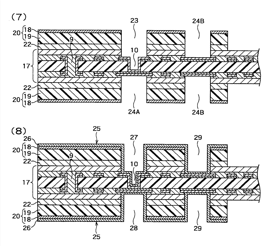
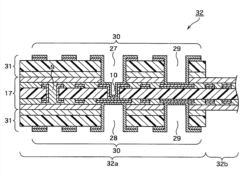
[0059] First, use Figure 1A to Figure 1C and figure 2 Next, a method for manufacturing the build-up type multilayer printed wiring board 32 having the via structure according to the embodiment of the present invention will be described.

[0060] Figure 1A to Figure 1C It is a process sectional drawing for demonstrating the ...


PUM


Abstract

Disclosed is a method of manufacturing build-up type multi-layer printed circuit boards having a stacked via structure allowing high-density component mounting. After forming a plated through via hole (9) and a plated via hole with a bottom (10) in a dual-side copper-clad laminate board, the copper foil on both sides of the dual-side copper-clad laminate board is patterned, resulting in a substrate with dual-side flexibility. Two cover lays (16) are prepared and laminated upon both sides of the substrate with dual-side flexibility. The laminating process is carried out under the following conditions: the interior of the plated through via hole (9) is completely filled with an adhesive agent derived by melting an adhesive agent layer (15) of the cover lay (16); and an air void (15a) may be allowed to occur, such that the interior of the plated via hole with the bottom (10) cannot be filled with the adhesive agent. After adhering a single-side copper-clad laminate board (20) to an insulator film (14) with an adhesive agent layer (22), laser working is used to remove the adhesive agent, and eliminate the air void (15a), within the plated via hole with the bottom (10), forming a step via hole such that the plated via hole with the bottom (10) becomes a lower hole.

Description

technical field [0001] This invention relates to the manufacturing method of a multilayer printed wiring board, More specifically, It is related with the manufacturing method of a build-up type multilayer printed wiring board. Background technique [0002] In recent years, miniaturization and higher functionality of electronic equipment such as portable information terminals such as mobile phones have been progressing. Therefore, there is an increasing demand for densification of printed wiring boards used in electronic equipment. [0003] Therefore, in order to mount electronic components on printed wiring boards at high density, research and development on build-up type multilayer flexible printed wiring boards has been actively carried out (for example, refer to Patent Document 1). The build-up type multilayer flexible printed wiring board uses a double-sided flexible printed wiring board or a multilayer flexible printed wiring board as a core substrate, and about 1 to 2...

Claims


Application Information

Patent Timeline
Patent Type & Authority Patents(China)
IPC IPC(8): H05K3/46
CPCH05K1/115H05K2201/0959H05K2201/09509H05K3/427H05K3/4652H05K2201/0394H05K2201/096
Inventor 松田文彦
Owner NIPPON MEKTRON LTD
Learn More