
The preparation method of multi-layer pcb board

A PCB board and core board technology, applied in the field of multi-layer PCB board preparation, can solve the problems of increased production cost, high product defect rate, and difficulty in precise copper thickness, so as to save production cost, reduce scrap rate, and reduce copper accurately. Effect

Inactive Publication Date: 2011-12-21
奥士康精密电路(惠州)有限公司
View PDF4 Cites 7 Cited by
  • Summary
  • Abstract
  • Description
  • Claims
  • Application Information

AI Technical Summary

Problems solved by technology

Multi-layer PCB boards often have yin and yang boards. The inner layer manufacturing process is complicated and the quality risks are relatively large. The conventional production process can easily lead to a high defect rate of the product, especially the copper thickness is difficult to be accurate, resulting in an increase in production costs.

Method used


Image

  • The preparation method of multi-layer pcb board
  • The preparation method of multi-layer pcb board

Examples


Embodiment Construction

[0015] The preparation method of the multi-layer PCB board of the present invention will be further described in detail below by taking the manufacture of a six-layer PCB board as an example.

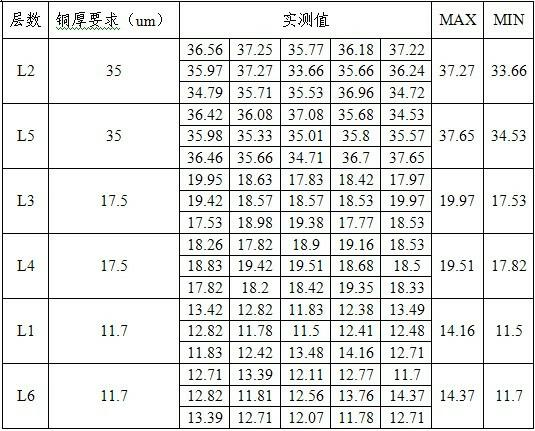
[0016] For the convenience of description, the outer layers of the six-layer PCB are marked as layers L1 and L6, and the middle layers are marked as layers L2, L3, L4, and L5. Among them, the target copper thickness of the inner layers L2 and L5 is 1OZ (ounce, 1oz=28.35 grams), and the target copper thickness of the L3 and L4 layers is 0.5OZ. The target copper thickness of the outer layers L1 and L6 is 1 / 3OZ.

[0017] The preparation method of this six-layer PCB board comprises:

[0018] step one:

[0019] Design and manufacture three double-sided core boards: the first core board, the second core board and the third core board. The upper and lower sides of the first core board are respectively used as the L1 layer and the L2 layer, the upper and lower sides of the second core board ...


PUM


Abstract

The invention relates to a method for preparing a multi-layer PCB (printed circuit board). The method comprises the following steps: providing a plurality of core boards according to the number of layers of the multi-layer PCB, wherein the initial copper thickness of the outward surfaces of the outward core boards is more than the target copper thickness; carrying out film stripping treatment on the plurality of core boards; carrying out oxidation treatment on the plurality of core boards subjected to film stripping treatment; using copper foils to carry out lamination treatment on the plurality of core boards subjected to oxidation treatment; and using etching solution to carry out micro-etching copper thinning treatment on the plurality of core boards subjected to lamination to ensure the copper thickness of the outward surfaces of the outward core boards to be equal to the target copper thickness. The formula of the etching solution comprises divalent copper ions (140-160g / l) and hydrogen chloride (3.65-10.95g / l); and the specific weight of the etching solution is 1200-1400g / l. The method has the following beneficial effects: by optimally adjusting the parameters of the micro-etching copper thinning process, the final copper reduction of the product can be very accurate, the inner layer is produced smoothly, the scrappage is reduced and the production cost is saved.

Description

technical field [0001] The present invention relates to a PCB (printed circuit board, printed circuit board) board, in particular to a preparation method of a multilayer PCB board. Background technique [0002] The current electronic products tend to be high-density and small-volume, so multi-layer PCB has a good market prospect. Most multi-layer PCB boards have yin and yang boards. The inner layer manufacturing process is complicated and the quality risks are relatively large. The conventional production process can easily lead to a high defect rate of the product, especially the copper thickness is difficult to be accurate, resulting in an increase in production costs. Contents of the invention [0003] Based on this, it is necessary to provide an improved multilayer PCB board and a manufacturing method thereof. [0004] A preparation method of a multilayer PCB board, comprising the steps of: providing a plurality of core boards according to the number of layers of the ...

Claims


Application Information

Patent Timeline
IPC IPC(8): H05K3/46
Inventor 孙益民贺波
Owner 奥士康精密电路(惠州)有限公司
Learn More