
Thick Film Spin Coating Method for Semiconductor Packaging

A technology of semiconductor and adhesive film, which is applied in the manufacture of semiconductor/solid-state devices, devices for coating liquid on the surface, and coatings, etc. It can solve the problems of slow consumption of edge solvents, long fusion time, and fast consumption of intermediate solvents, etc., to achieve saving The cost of equipment transformation and the effect of simple process debugging

Active Publication Date: 2011-11-30
SHENYANG KINGSEMI CO LTD
View PDF5 Cites 12 Cited by
  • Summary
  • Abstract
  • Description
  • Claims
  • Application Information

AI Technical Summary

Problems solved by technology

[0002] At present, the known thick glue coating process for semiconductor packaging requires secondary glue coating. The usual glue coating method will cause the middle thickness of the wafer to be higher than the thickness of the two sides after the second glue coating. This is because the second glue coating is different from the first glue coating. In the film forming process, the negative film of the first coating and film forming process is a wafer, which will not undergo secondary fusion with the photoresist. However, the secondary coating process is based on the previous film. The glue-coated film will have a secondary fusion physical effect with the first glue-coated film, especially the glue in the center. The glue in the middle of the wafer will fuse with the previous film for the longest time, resulting in the consumption of intermediate solvents during glue coating. Faster, the edge solvent consumption is slower, the concentration gradient of the solvent is poor, and the middle of the glue is obviously behind the two sides

Method used


Image

  • Thick Film Spin Coating Method for Semiconductor Packaging
  • Thick Film Spin Coating Method for Semiconductor Packaging
  • Thick Film Spin Coating Method for Semiconductor Packaging

Examples


Embodiment 1

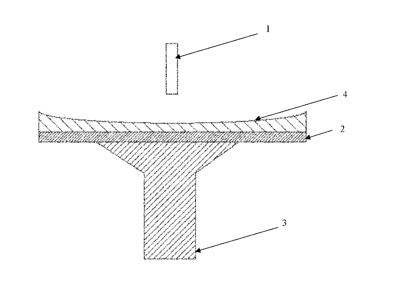
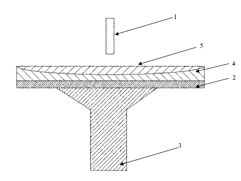
[0019] In this embodiment, when applying glue for the first time, the viscosity of the positive photoresist is 300 centipoise, and the rotation speed of the vacuum chuck is 1200 rpm; when applying glue for the second time, the viscosity of the positive photoresist is 300 centipoise , the rotation speed of the vacuum chuck is 1200rpm; the distance between the outlet of the dripping pipeline 1 and the wafer 2 is 15mm, and the diameter of the wafer 2 is 8 inches.

Embodiment 2

[0021] In this embodiment, when applying glue for the first time, the viscosity of the negative photoresist is 4000 centipoise, and the rotation speed of the vacuum chuck is 1500 rpm; when applying glue for the second time, the viscosity of the negative photoresist is 4000 centipoise , the rotation speed of the vacuum chuck is 1600rpm; the distance between the outlet of the dripping pipeline 1 and the wafer 2 is 10mm, and the diameter of the wafer 2 is 12 inches.

Embodiment 3

[0023] In this embodiment, when applying glue for the first time, the viscosity of the negative photoresist is 1500 centipoise, and the rotation speed of the vacuum chuck is 3000 rpm; when applying glue for the second time, the viscosity of the negative photoresist is 1500 centipoise , the rotation speed of the vacuum chuck is 2800rpm; the distance between the outlet of the dripping pipeline 1 and the wafer 2 is 20mm, and the diameter of the wafer 2 is 8 inches.

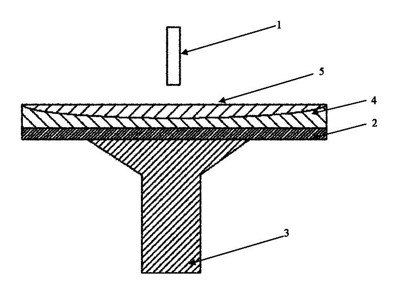
[0024] The results of the examples show that the present invention achieves that the center of the glue-coated film is slightly thinner and the edge is slightly thicker for the first time through the control of the glue-spraying speed and the glue-spinning speed through the central glue-dropping and rotating glue-coating. The invention realizes that the center of the second glue coating film is slightly thicker and the edge is slightly thinner through the control of the glue spreading speed and the glue throwing speed...


PUM


Abstract

The invention relates to the field of semiconductors, and specifically relates to a spin-coating method for forming a thick film for packaging a semiconductor through two stages of special spin-coating on a semiconductor wafer. Specifically, a special two-stage coating method is adopted for packaging the semiconductor. Through complementation of different film thicknesses and forms of the films coated in the two stages, homogeneity of the thick film for packaging is achieved. In the first coating stage, the cement is coated in a manner that the film turns thicker from the center to the edge, that is to say, the cement is coated in a manner that a cross section through the central point is in an inferior pattern. In the second coating stage, the cement is coated in a manner that the film turns thinner from the center to the edge, that is to say, the cement is coated in a manner that a cross section through the central point is in a convex pattern. With the two-stage special coating method provided by the invention, a film coating requirement of thick high-viscosity film packaging technology is satisfied, and a defect of prior two-stage coating technologies is solved.

Description

technical field [0001] The present invention relates to the field of semiconductors, in particular to a spin coating method for obtaining a thick adhesive film for thick semiconductor packaging through two special coating spin coating methods on a semiconductor wafer, in particular to a thick adhesive coating method for semiconductor packaging The special two-time glue coating method complements each other through two different film thicknesses and forms to achieve the uniformity of the thick glue film for final packaging. Background technique [0002] At present, the known thick glue coating process for semiconductor packaging requires secondary glue coating. The usual glue coating method will cause the middle thickness of the wafer to be higher than the thickness of the two sides after the second glue coating. This is because the second glue coating is different from the first glue coating. In the film forming process, the negative film of the first coating and film formin...

Claims


Application Information

Patent Timeline
Patent Type & Authority Applications(China)
IPC IPC(8): B05C11/08H01L21/56
Inventor 王阳胡延兵
Owner SHENYANG KINGSEMI CO LTD
Learn More