
Flexible printed board and method of manufacturing same

A flexible printing and circuit board technology, applied in the fields of printed circuit manufacturing, printed circuit, printed circuit, etc., can solve the problems that the flexibility of the flexible printed circuit board cannot be fully improved, and the influence of the bending of the conductive resin layer is not discussed, etc., to achieve Improves bendability and relieves stress concentration

Active Publication Date: 2011-10-12
FUJIKURA LTD
View PDF5 Cites 12 Cited by
  • Summary
  • Abstract
  • Description
  • Claims
  • Application Information

AI Technical Summary

Problems solved by technology

[0004] In the above-mentioned flexible printed circuit boards, the influence of the conductive resin layer of the electromagnetic shielding layer formed by screen printing on the flexibility is not discussed.
[0005] For this reason, there are cases where the flexibility of the flexible printed circuit board cannot be sufficiently improved.

Method used


Image

  • Flexible printed board and method of manufacturing same
  • Flexible printed board and method of manufacturing same
  • Flexible printed board and method of manufacturing same

Examples


Embodiment 1

[0081] In Example 1, ten samples (samples 1 to 10) of the flexible printed wiring board having the same structure as the above-mentioned embodiment were produced.

[0082]In the samples of Example 1, the insulating substrate was made of polyimide, the circuit wiring was made of copper, the circuit protection layer was made of a film, the shielding conductive layer was made of silver paste, and the insulating ink was used Constitutes a shielding insulation layer. In addition, the adhesive layer of the cover film was made of an adhesive made of epoxy resin, and the insulating film was made of polyimide. In addition, the binder of the silver paste uses a polyester resin with a viscosity of about 200 [dPa·S at 25°C] to 300 [dPa·S at 25°C]. In addition, the insulating ink uses a polyester resin with a viscosity of about 50 [dPa·S at 25°C] to 150 [dPa·S at 25°C].

[0083] In the samples of Example 1, the thickness of the insulating substrate was set to 12.5 [μm], the thickness of ...

Embodiment 2~5

[0100] In Examples 2 to 5, as shown in Table 1, 10 tensile elastic moduli E 2 Samples having the same structure as in Example 1 except for 1.9 [GPa], 2.4 [GPa], 2.88 [GPa], and 3.1 [GPa], respectively.

[0101] About the samples of these Examples 2-5, the sliding test was performed by the same procedure as Example 1. The result for embodiment 2~5 is in table 1 and Figure 9 shown in .

Embodiment 6

[0103] In Example 6, 10 samples (samples 1 to 10) having the same structure as in Example 1 were prepared except that the thickness of the adhesive layer of the coating was 30 [μm]. For these samples of Example 6, a sliding test was performed in the same manner as in Example 1. For the result of embodiment 6 in table 2 and Figure 10 shown in . in addition, Figure 10 The graph of is plotted the number of cycles at the time of wire breakage of samples 1 to 10 of Example 6 (the same applies to Examples 7 to 10 and Comparative Examples 3 and 4).

[0104] 【Table 2】

[0105]


PUM


Abstract

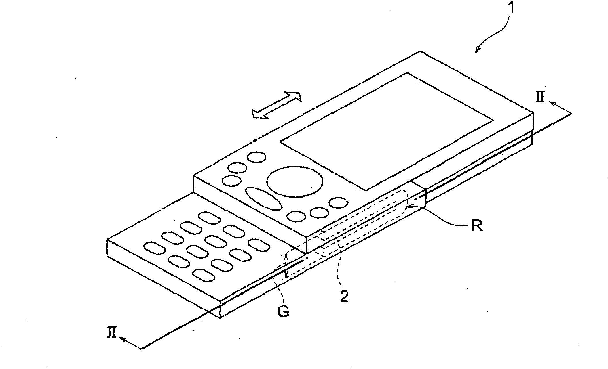
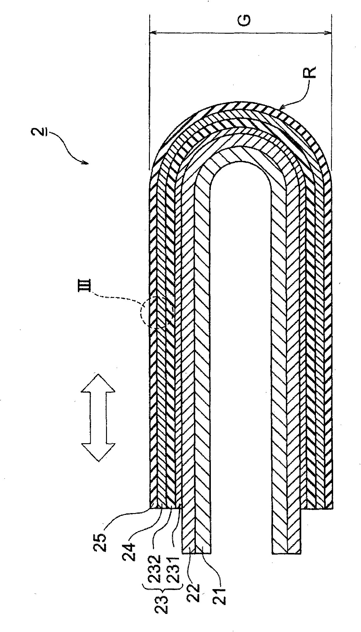
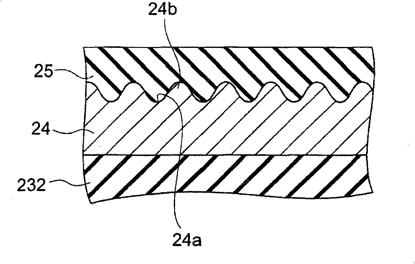
The invention provides a flexible printed board improved in bendability and a method of manufacturing the same. The flexible printed board 2 comprises: an insulating substrate 21; a circuit wiring 22 laid on the insulating substrate 21; a circuit protection layer 23 laid on the circuit wiring 22; a shield conductive layer 24 laid on the circuit protection layer 23; and a shield insulating layer 25 laid on the shield conductive layer 24, and is characterized by meeting the following Expression (1). 0.75<=E2 / E1<=1.29... Expression (1) Note that E1 denotes the tensile elastic modulus of the shield conductive layer 24 and E2 denotes the tensile elastic modulus of the shield insulating layer 25.

Description

technical field [0001] The present invention relates to a flexible printed circuit board that can be bent with a narrow gap (small radius) and its manufacturing method. Background technique [0002] It is known that the thickness of the conductive resin layer of the electromagnetic wave shielding layer is 1 [μm] to 20 [μm], and the thickness of the insulating resin layer of the electromagnetic wave shielding layer is 3 [μm] to 20 [μm]. A flexible printed circuit board (for example, refer to Patent Document 1). [0003] [Patent Document 1] JP Unexamined Publication No. 2008-98613 [0004] In the flexible printed wiring board described above, the influence of the conductive resin layer of the electromagnetic wave shielding layer formed by screen printing on the flexibility is not considered. [0005] For this reason, the flexibility of the flexible printed circuit board may not be sufficiently improved. Contents of the invention [0006] The object of the problem to be so...

Claims


Application Information

Patent Timeline
Patent Type & Authority Applications(China)
IPC IPC(8): H05K1/02H05K3/00
CPCH05K1/0218H05K1/028H05K3/1216H05K2201/0373Y10T29/49124
Inventor 渡边裕人
Owner FUJIKURA LTD
Learn More