Wafer-bonding-based triple-junction solar cell and preparation method thereof

A solar cell, wafer bonding technology, applied in circuits, photovoltaic power generation, electrical components, etc., can solve problems such as the difficulty of triple junction cells

Inactive Publication Date: 2011-09-14
SUZHOU INST OF NANO TECH & NANO BIONICS CHINESE ACEDEMY OF SCI
View PDF8 Cites 30 Cited by
  • Summary
  • Abstract
  • Description
  • Claims
  • Application Information

AI Technical Summary

Problems solved by technology

However, it is extremely challenging to grow a high-quality epitaxial layer with a lattice mismatch of 2%, and it is very difficult to prepare triple-junction cells with a lattice mismatch

Method used


Image

  • Wafer-bonding-based triple-junction solar cell and preparation method thereof
  • Wafer-bonding-based triple-junction solar cell and preparation method thereof
  • Wafer-bonding-based triple-junction solar cell and preparation method thereof

Examples


Embodiment Construction

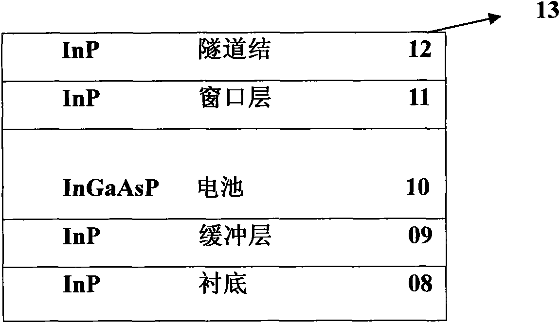
[0072] Aiming at the deficiencies of the prior art, the inventor of this case has designed a GaInP / GaAs / InGaAsP triple-junction solar cell based on wafer bonding after long-term research and practice. Combined, the bandgap combination is 1.90eV, 1.42eV, ~1.00eV, and a balance point is found to reduce the battery current mismatch and reduce the difficulty of material growth.

[0073] The triple-junction solar cell based on wafer bonding that the present invention relates to mainly includes two types of structures:

[0074] The first type of structure is that both the GaInP / GaAs double-junction cell and the InGaAsP single-junction cell use a P-type substrate, and a tunnel junction is grown on the window layer of the InGaAsP single-junction cell to realize the conversion from N-type to P-type. Methods as below:

[0075] (1) GaInP / GaAs double junction cell is grown by MOCVD method, its structure is as follows figure 1 Shown:

[0076] (1) growing a P-type GaAs buffer layer 02 on...


PUM


Abstract

The invention relates to a wafer-bonding-based triple-junction solar cell and a preparation method thereof. The solar cell comprises a GaInP/GaAs double-junction cell and an InGaAsP single-junction cell of which the lattices are matched with each other, wherein the two cells are connected in series in a way of wafer bonding. The preparation method comprises the following steps of: sequentially growing and forming the GaInP/GaAs double-junction cell and the InGaAsP single-junction cell by a metal organic chemical vapor deposition (MOCVD) method and the like; thinning, polishing and cleaning the bonding face of the GaInP/GaAs double-junction cell, and bonding the GaInP/GaAs double-junction cell with the InGaAsP cell; and making an upper electrode and a lower electrode respectively form the target product. A band gap combination of 1.90eV, 1.42eV and 1.00eV can be formed; the growing difficulty of materials is reduced; solar spectrum is fully used; current mismatch between subcells and heat loss in a photoelectric conversion process are reduced; the internal quantum efficiency of a 1.00eV cell is improved at the same time; and then the cell efficiency is improved.

Description

technical field [0001] The invention specifically relates to a triple-junction solar cell based on wafer bonding and a preparation method thereof. The triple-junction solar cell can fully utilize the solar spectrum and has high cell efficiency. Background technique [0002] In the field of solar cells, the GaInP / GaAs / Ge triple-junction cell is currently the most researched and mature system. The highest conversion efficiency of this material system is 32-33% under one sun. The Ge battery in the triple-junction battery covers a wider spectrum, and its short-circuit current can reach twice that of the other two-junction batteries. Due to the restriction of the series connection of the three-junction batteries, the energy of the solar spectrum corresponding to the Ge battery is not fully converted and utilized. Therefore, there is still room for improvement in the efficiency of the triple-junction cell. The most intuitive idea is to insert a material with a bandgap of ~1.00eV ...

Claims


Application Information

Patent Timeline
Patent Type & Authority Applications(China)
IPC IPC(8): H01L31/0352H01L31/06H01L31/18
CPCY02E10/50Y02E10/544Y02P70/50
Inventor 李奎龙董建荣陆书龙赵勇明杨辉
Owner SUZHOU INST OF NANO TECH & NANO BIONICS CHINESE ACEDEMY OF SCI
Why Eureka
Try Eureka