
Method for measuring low background carrier concentration by utilizing optical excitation differential capacitance method

A technology of carrier concentration and differential capacitance, which is applied in the direction of material capacitance, measuring devices, scanning probe microscopy, etc., can solve the problem of inability to apply semiconductor integrated device detection, limited sensitive response range of differential capacitance, and lack of quantitative detection ability and other problems, to achieve the effects of significant changes in experimental characteristics, easy judgment and implementation, and high precision

Active Publication Date: 2011-09-07
SHANGHAI INST OF TECHNICAL PHYSICS - CHINESE ACAD OF SCI
View PDF2 Cites 13 Cited by
  • Summary
  • Abstract
  • Description
  • Claims
  • Application Information

AI Technical Summary

Problems solved by technology

[0004] The electrochemical capacitance-bias ECV method can provide the carrier distribution in the depth direction of the sample with high accuracy, and the resolution can be down to the nanometer level, and its detectable concentration range can be as low as 10 in principle. 12 cm -3 ; but limited by the Debye length (P.Blood, Semicond.Sci.Technol.1 (1986) 7-27), low concentration measurement requires an increase in the thickness of the region, such as 1 × 10 15 cm -3 carrier concentration, the Debye length corresponding to the Schottky barrier with a height of only 0.1eV has reached 0.32 microns; Influenced by factors such as deviation, the error of ECV detection also increases greatly, so there is no ECV method with 1×10 15 cm -3 Reports of reliable applications on multilayer structures in the carrier concentration region below
In addition, the ECV method requires a certain size (diameter in millimeters) of the lateral etching surface, which cannot be applied to the detection of designated functional blocks of semiconductor integrated devices or array devices.
[0005] The basic principle of Scanning Capacitance Microscopy (SCM) is similar to the ECV method, but in order to obtain two-dimensional spatial resolution, nanoprobes are used as moving electrodes, and the sensitive response range of its differential capacitance is limited. Reliable measurements in the range of 10 15 ~10 19 cm -3 , does not have the ability to quantitatively detect lower concentrations

Method used


Image

  • Method for measuring low background carrier concentration by utilizing optical excitation differential capacitance method
  • Method for measuring low background carrier concentration by utilizing optical excitation differential capacitance method
  • Method for measuring low background carrier concentration by utilizing optical excitation differential capacitance method

Examples


Embodiment Construction

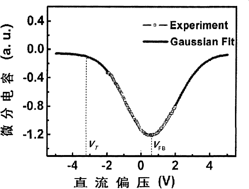
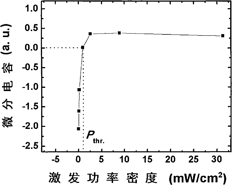
[0037] The substantive features and relative advantages of the present invention are further described below by measuring the carrier concentration in the InGaAs non-doped absorption region in the InGaAs / InP avalanche photodiode structure, but the present invention is not limited, that is, the present invention is by no means limited to this embodiment.

[0038] The InGaAs / InP avalanche photodiode structure applicable to the present invention includes: on the InP substrate, an N-type InP bottom electrode layer, an unintentionally doped InGaAs absorption layer, an n-type InGaAsP layer, an n-type InP layer, an unintentionally doped InP multiplication layer and P-type InP layer.

[0039] The diode structure is a vertical distribution structure along the material growth direction, so it is necessary to prepare a smooth section through the unintentionally doped InGaAs absorption layer as the measurement surface, which can take advantage of the crystal characteristics of InP-based se...


PUM

PropertyMeasurementUnit
Thicknessaaaaaaaaaa

Abstract

The invention discloses a method for measuring the low background carrier concentration in a semiconductor material device, and the method comprises the following steps: measuring the flat belt voltage on the surface of a region to be measured and the differential capacitance response under the optical excitation condition; establishing a numerical value model of the region to be measured and theadjacent region; and comparing the surface differential capacitance under the optical excitation condition of the region to be measured of the numerical value model and the practical measurement so as to determine the balanced carrier concentration. The method disclosed by the invention is suitable for the accurate measurement of the specific function region in the semiconductor material or device provided with a complicated structure, and the background carrier concentration of the specific function region is lower than 1015cm<-3>; and method can be used for detecting a single microcosmic block in an integrated or array device.

Description

technical field [0001] The invention relates to a method for measuring characteristic parameters of semiconductor material devices, in particular to the measurement of extremely low background carrier concentration in a specific region of a semiconductor material device. It belongs to the field of semiconductor material characterization. Background technique [0002] Semiconductor devices realize their electrical or photoelectric functions through the transport, transition and relaxation of free electrons, that is, carriers. Therefore, measuring and controlling the carrier concentration in each functional area is one of the important contents of semiconductor materials and device processes. In some specific regions of semiconductor devices, such as the absorption region of semiconductor photodetectors, a very low background carrier concentration (≤10 15 cm -3 ) to obtain key performances such as low noise, high mobility and long minority carrier lifetime; for this purpose,...

Claims


Application Information

Patent Timeline
IPC IPC(8): G01N27/22G01Q60/46
Inventor 李天信夏辉陆卫殷豪黄文超王文娟胡伟达李宁陈平平李志峰陈效双
Owner SHANGHAI INST OF TECHNICAL PHYSICS - CHINESE ACAD OF SCI
Learn More