
Fairlead structure for Bipolar circuit and manufacturing method thereof

A bipolar circuit and manufacturing method technology, which is applied to circuits, semiconductor/solid-state device manufacturing, electrical components, etc., can solve the problems of increasing the longitudinal width of the lead hole, reducing the manufacturing cost, and worsening the coverage, so as to improve the effective die. number, cost reduction, and the effect of stabilizing bottom size

Inactive Publication Date: 2013-09-04
HANGZHOU SILAN INTEGRATED CIRCUIT
View PDF0 Cites 0 Cited by
  • Summary
  • Abstract
  • Description
  • Claims
  • Application Information

AI Technical Summary

Problems solved by technology

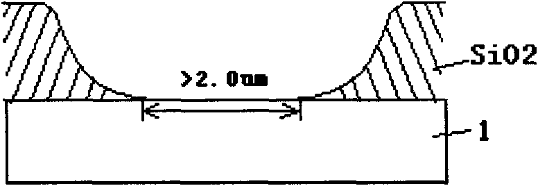
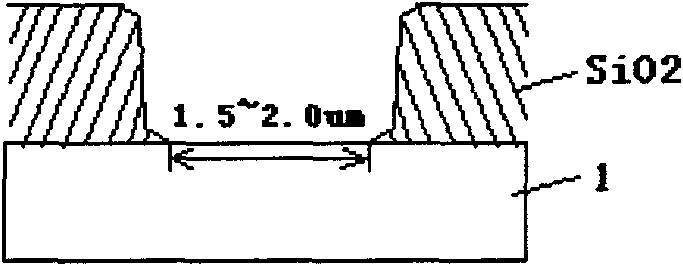
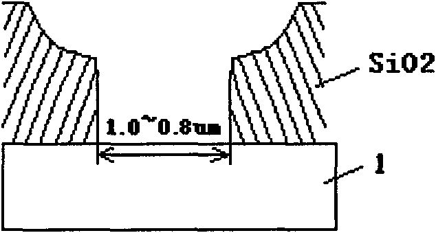
[0008] The 1.0-1.2um process platform is developed on the basis of the 1.5um process platform equipment group. The lead hole rules of each lithography layer are further reduced compared with the 1.5um process, and the bottom requires a smaller lateral erosion allowance. With the shrinkage of the lead hole and the thickness of the hole medium Increase (to meet the high-voltage process requirements of some small rule products and improve the withstand voltage of parasitic MOS), the aspect ratio of the lead hole will be relatively larger, and the lead hole made by the dry and wet etching process will have poor step coverage after sputtering aluminum. Improvement; but the use of 0.8um process platform equipment group to process the bowl mouth process, the cost is relatively high, which is not conducive to the reduction of manufacturing costs

Method used


Image

  • Fairlead structure for Bipolar circuit and manufacturing method thereof
  • Fairlead structure for Bipolar circuit and manufacturing method thereof
  • Fairlead structure for Bipolar circuit and manufacturing method thereof

Examples


Embodiment Construction

[0052] The content of the present invention will be further described below in conjunction with the accompanying drawings. Taking the motor-driven ASIC manufactured on the 1.2um15V process platform as an example, the method for manufacturing the lead hole structure of the bipolar circuit includes the following steps:

[0053] (1) On the silicon substrate 1 provided with the polar region, a bottom layer of thermally grown silicon oxide film layer 2 is formed, and the bottom layer of thermally grown silicon oxide film layer is formed in one of the following two ways: (A) on the silicon base layer Form the P-type doped region and the N-type doped region in the bipolar circuit by implanting with glue, and keep the implanted masking thermal oxide layer As the bottom layer of thermally grown silicon oxide film layer (B); after forming the P-type doped region and the N-type doped region in the bipolar circuit by a diffusion process on the silicon base layer, the newly formed The b...


PUM


Abstract

A manufacturing method of a fairlead structure for a bipolar circuit comprises the following steps of: (1) forming a bottom silicon oxide thin film layer on a silicon substrate provided with a pole zone; (2) forming a top silicon oxide thin film layer on the bottom silicon oxide thin film layer by deposition; (3) depositing a silicon nitride thin film layer on the top silicon oxide thin film layer; (4) and conducting photoetching and etching on a pre-etched zone of the silicon nitride thin layer to form a fairlead. Based on the 1.5mum technique platform equipment set, the method of the invention manufactures a fairlead structure for a bipolar circuit, which satisfies 1.0mum to 1.2mum technique platform, and effectively solves the step metal cover problem of the fairlead when the technique platform is close to sub-micron level.

Description

technical field [0001] The invention relates to the technical field of integrated circuit manufacturing technology, in particular to the manufacturing technology and manufacturing method of lead holes adjacent to submicron small regular bipolar circuits. Background technique [0002] The size of the lead hole in a bipolar circuit is determined by the minimum line width of the process platform, and the aluminum step coverage of the lead hole is an important indicator that affects the symmetry and reliability of the integrated circuit. [0003] For bipolar circuits manufactured on 3.0um and above process platforms, the lead hole rules of each photolithography layer are relatively large, and the allowable lateral erosion allowance is relatively large. At the same time, the aspect ratio of the lead hole is relatively small. Usually, pure wet etching process is used. After etching, the step of the lead hole is a large bowl shape (see figure 1 ), the steps are covered well after ...

Claims


Application Information

Patent Timeline
Patent Type & Authority Patents(China)
IPC IPC(8): H01L23/48H01L23/00H01L21/768H01L21/314H01L21/3105
Inventor 李小锋陈元金杨彦涛张佼佼
Owner HANGZHOU SILAN INTEGRATED CIRCUIT
Learn More