
Method for manufacturing serial uniwafer integrated multi-junction thin film solar cell

A solar cell, monolithic integration technology, applied in the direction of final product manufacturing, sustainable manufacturing/processing, circuits, etc., can solve the problems of heavy solar cells, inability to meet high-voltage applications, and inability to meet applications, and achieve high-efficiency photoelectric conversion. , with market competitiveness, the effect of weight reduction

Inactive Publication Date: 2013-05-01
SUZHOU INST OF NANO TECH & NANO BIONICS CHINESE ACEDEMY OF SCI
View PDF2 Cites 0 Cited by
  • Summary
  • Abstract
  • Description
  • Claims
  • Application Information

AI Technical Summary

Problems solved by technology

[0003] Existing multi-junction solar cells are single discrete structures with an output voltage of only a few volts, which cannot meet high-voltage applications; and due to the use of hard substrates, the cells are rigid and cannot meet applications on curved surfaces such as balloons and airships; In addition, the weight of the solar cell is relatively large, and the epitaxial layer is only about 10 μm effective, while the supporting substrate is 300-500 μm thick, making more than 95% of the weight of the traditional solar cell ineffective.

Method used


Image

  • Method for manufacturing serial uniwafer integrated multi-junction thin film solar cell
  • Method for manufacturing serial uniwafer integrated multi-junction thin film solar cell
  • Method for manufacturing serial uniwafer integrated multi-junction thin film solar cell

Examples


Embodiment Construction

[0032] Below will further illustrate the present invention with embodiment in conjunction with accompanying drawing:

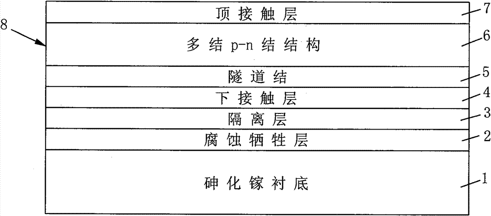
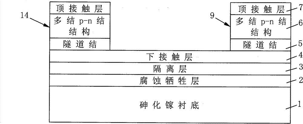
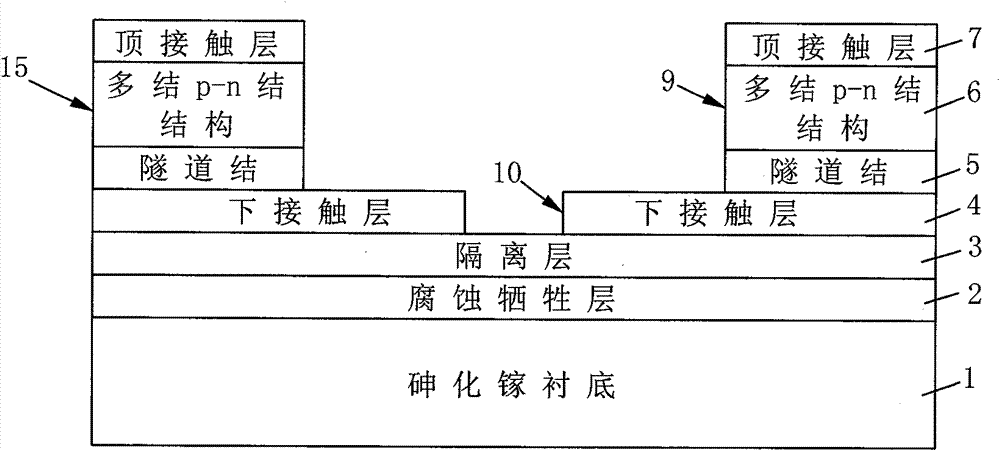
[0033] The tandem monolithic integrated multi-junction thin-film solar cell of this embodiment is mainly composed of the following parts: 1. Substrate, 2. Isolation layer, 3. Lower contact layer, 4. Tunnel junction, 5. Multi-junction p-n junction Structure, 6. Top contact layer, 7. Passivation insulating layer, 8. Electrical connection layer.

[0034] The manufacturing method of this tandem monolithic integrated multi-junction thin film solar cell mainly includes the following steps:

[0035] 1. If figure 1 As shown, an etching sacrificial layer 2 is grown on a gallium arsenide (GaAs) substrate 1 by molecular beam epitaxy or metal organic chemical vapor deposition, and the etching sacrificial layer 2 is made of aluminum arsenide (AlAs) material. At the same time, a multi-junction solar cell epitaxial material 8 is deposited on the etching sacrificial layer 2...


PUM


Abstract

The invention relates to the manufacturing field of a serial uniwafer integrated multi-junction thin film solar cell. The manufacturing method comprises the following steps: depositing a multi-junction p-n junction serial solar cell epitaxy material comprising at least an insulating layer, a lower contact layer, a tunnel junction, a multi-junction p-n junction structure and a top contact layer which are grown upwards from the substrate and are connected sequentially by utilizing a molecular epitaxy or metallorganics chemical vapor deposition method; corroding to form a lower contact layer table board by utilizing a photoetching technology and an etching technology, and etching the corrosion table board to the lower isolating layer; growing and passivating the insulating layer is at the frontage of the solar cell epitaxy material by utilizing a deposition method, and manufacturing an electrode window and a light in window by utilizing the photoetching and etching technologies; and manufacturing an electric connecting layer on the electrode window and the passivated insulating layer by utilizing the photoetching and film coating technologies, and forming the electric connection between a top contact layer and the lower contact layer through a stripping technology and an annealing process. The solar cell has the characteristics of high efficiency, high-voltage output, light weight and flexibility.

Description

technical field [0001] The invention relates to the manufacturing field of a series monolithic integrated multi-junction thin film solar cell. Background technique [0002] Existing mass-produced solar cells are mainly made of materials such as polysilicon and amorphous silicon. Since the bandgap of silicon is only 1.1eV, and it is an indirect bandgap semiconductor material, the photoelectric conversion efficiency is not high, only about 16%. If the multi-junction form is used to absorb sunlight through the multi-junction structure, the efficiency can be greatly increased, which can reach more than 40%. [0003] Existing multi-junction solar cells are single discrete structures with an output voltage of only a few volts, which cannot meet high-voltage applications; and due to the use of hard substrates, the cells are rigid and cannot meet applications on curved surfaces such as balloons and airships; In addition, the weight of the solar cell is relatively large, and the ep...

Claims


Application Information

Patent Timeline
Patent Type & Authority Patents(China)
IPC IPC(8): H01L31/18
CPCY02P70/521Y02P70/50
Inventor 黄寓洋张耀辉殷志珍崔国新张宇翔冯成义李文
Owner SUZHOU INST OF NANO TECH & NANO BIONICS CHINESE ACEDEMY OF SCI
Learn More