
Formation method for grid structure

A technology of gate structure and graphics, which is applied in the direction of semiconductor devices, etc., can solve the problem of low reliability of gate structure

Active Publication Date: 2011-08-10
SHANGHAI HUAHONG GRACE SEMICON MFG CORP
View PDF4 Cites 0 Cited by
  • Summary
  • Abstract
  • Description
  • Claims
  • Application Information

AI Technical Summary

Problems solved by technology

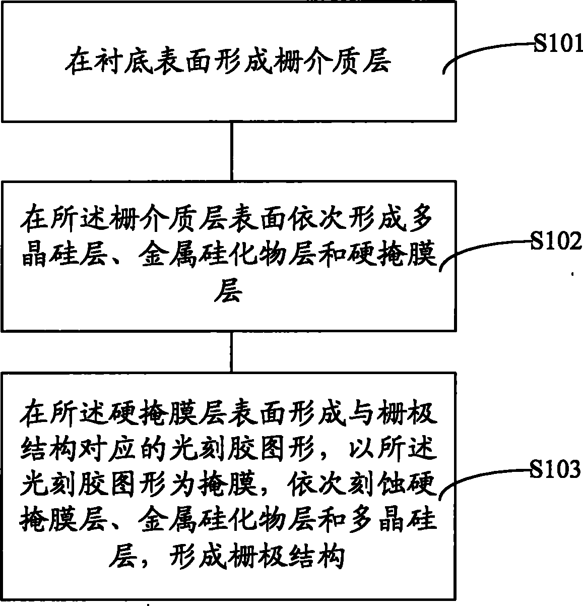
[0009] The above etching process usually uses CF-containing 4 , Cl and He plasma etching, too strong plasma etching will cause damage to the polysilicon layer when etching the metal silicide layer. After the next step, the process penetrates the gate dielectric layer to form etch pits (Pits) on its surface, and the plasma Weak bulk etching will form some impurities in the polysilicon layer and finally form impurities on the surface of the dielectric layer. The reliability of the gate structure formed by the above plasma etching process is low.

Method used


Image

  • Formation method for grid structure
  • Formation method for grid structure
  • Formation method for grid structure

Examples


Embodiment Construction

[0018] The existing gate structure formation process will use plasma etching, the plasma etching is too strong, the etching metal silicide layer will cause damage to the polysilicon layer, and finally form etch pits (Pits) on the surface of the gate dielectric layer, resulting in gate The electrode structure fails; while the weak plasma etching will form some impurities in the polysilicon layer, and finally form the residual impurities on the surface of the dielectric layer, which will degrade the performance of the gate structure. Aiming at the defects formed in the formation process of the above-mentioned gate structure, those skilled in the art usually optimize by adjusting parameters such as etching power and etching time, but due to the presence of CF 4 It is difficult to optimize the plasma etching by the above optimization method. If the etching power is high or the etching time is long, etch pits will be formed, and if the etching power is small or the etching time is s...


PUM

PropertyMeasurementUnit
thicknessaaaaaaaaaa
thicknessaaaaaaaaaa
thicknessaaaaaaaaaa

Abstract

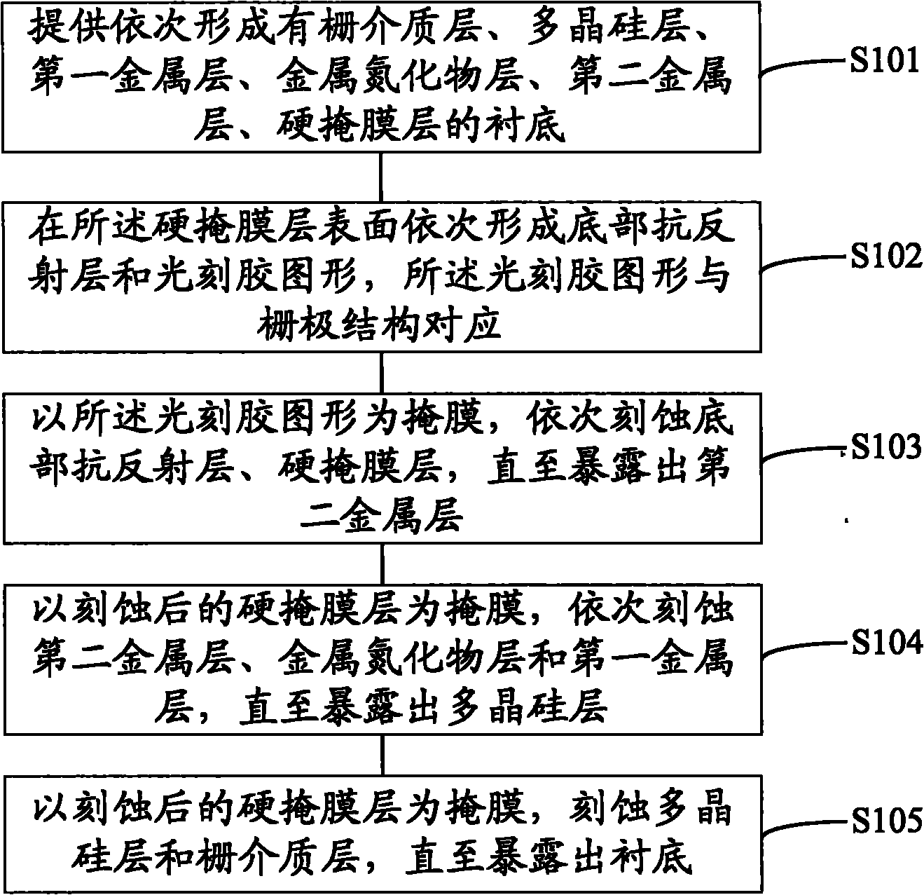
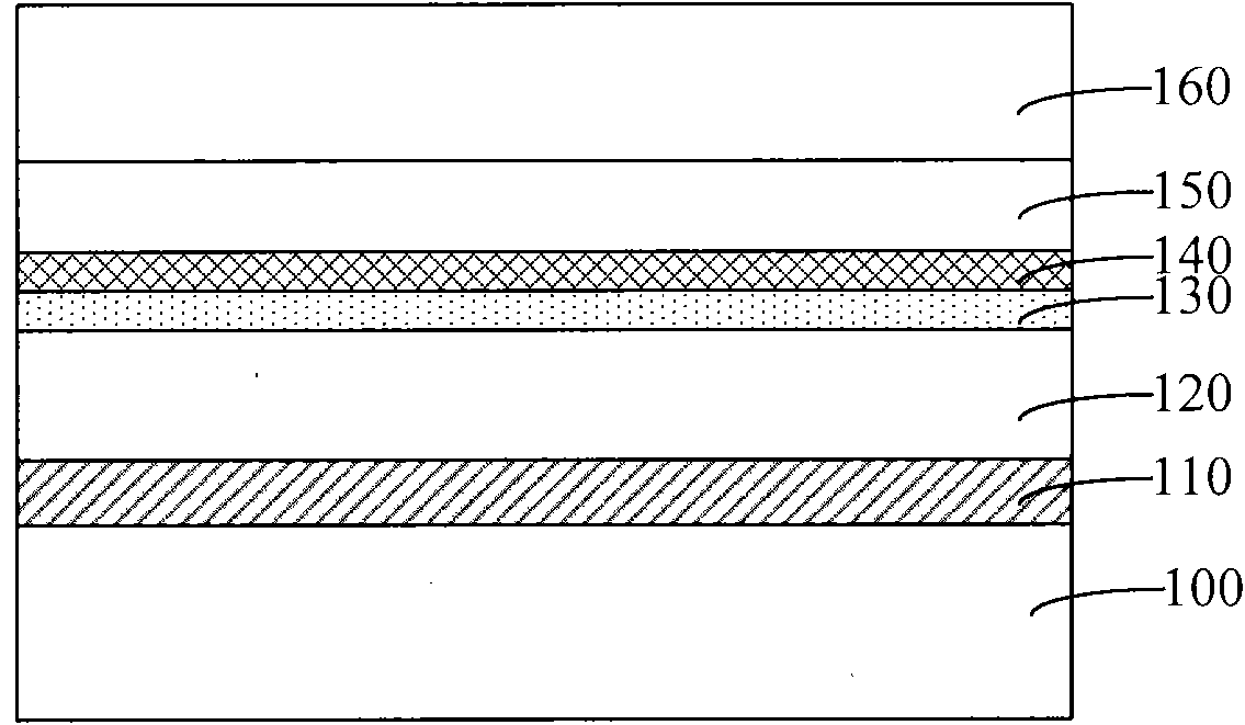
The invention relates to a formation method for a grid structure, which comprises the following steps: providing a substrate on which a grid dielectric layer, a polycrystalline silicon layer, a first metal layer, a metal nitride layer, a second metal layer and a hard masking film layer are formed; sequentially forming a bottom anti-reflection layer and a photoresist pattern on the surface of the hard masking film layer, wherein the photoresist pattern corresponds to the grid structure; taking the photoresist pattern as a masking film to sequentially etch the bottom anti-reflection layer and the hard masking film layer till the second metal layer is exposed; taking the etched hard masking film layer as the masking film, and adopting Cl2, NF3, O2 as etching gas, wherein the volume ratio of Cl2 and NF3 is less than 2, and sequentially etching the second metal layer, the metal nitride layer and the first metal layer till the polycrystalline silicon layer is exposed. No etched pits and impurities are left on the surface of the grid structure formed by the formation method.

Description

technical field [0001] The invention relates to the field of semiconductor manufacturing, in particular to a gate structure forming method. Background technique [0002] At present, VLSI has developed to an integration level of more than 100,000 components per single chip. In addition to requiring new circuit design, new device structure and technology, etc., this circuit must further reduce the number of devices. Geometry. [0003] As the aggregate size decreases, Al and polysilicon, which are usually used as low-resistance gates, have a series of problems. For example, for Al, Al is easy to infiltrate in silicon, so there is a short circuit caused by Al infiltration; for polysilicon In terms of its high resistivity (about 10 3 Ωcm), when the line width is reduced to 1 micron, its time constant RC is relatively large, which will affect the speed of the circuit. [0004] In order to solve this problem, the low-resistance gate formation process has become one of the key ma...

Claims


Application Information

Patent Timeline
Patent Type & Authority Applications(China)
IPC IPC(8): H01L21/28
Inventor 任晓辉奚裴齐龙茵
Owner SHANGHAI HUAHONG GRACE SEMICON MFG CORP
Learn More