Single board shielding structure, implementation method thereof, single board and communication equipment
A technology of shielding structure and realization method, applied in the field of communication, can solve the problems of large space occupation, unfavorable repair, and high thickness, and achieve the effects of convenient installation, reducing the risk of short circuit, and reducing thickness
- Summary
- Abstract
- Description
- Claims
- Application Information
AI Technical Summary
Problems solved by technology
Method used
Image
Examples
Embodiment 1
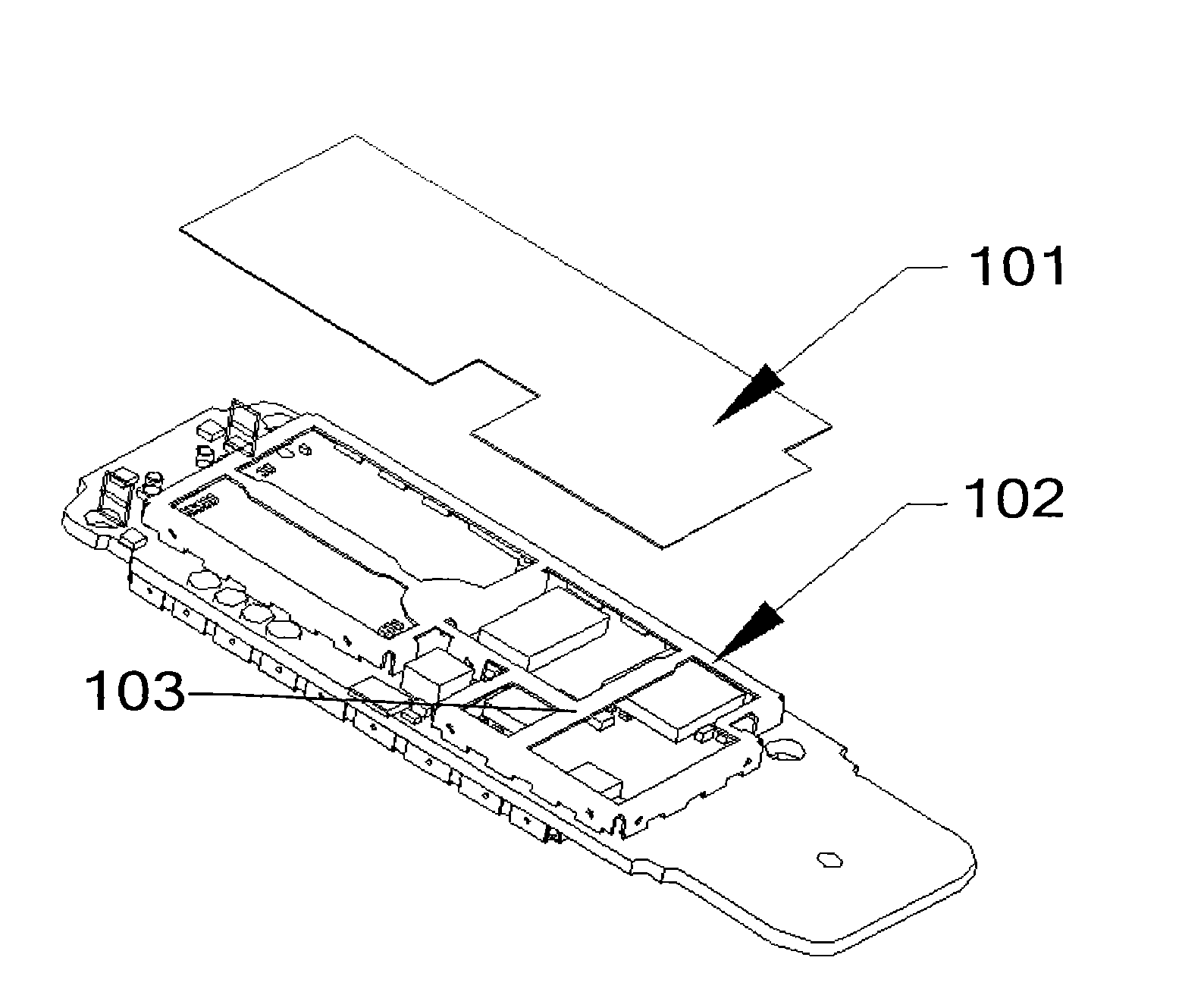
[0030] Embodiment 1 of the present invention provides a veneer shielding structure, which is used to shield radiation sources in a veneer, such as figure 2 As shown, the shielding structure includes:
[0031] Shielding frame 102 and shielding film 101;
[0032] The shielding frame 102 is used to be fixedly arranged on the single board by welding, and the shielding frame is provided with partition ribs 103, and the partition ribs 103 divide the inside of the shielding frame 102 into multiple spaces, which can separate each radiation on the single board. source, the shielding film 101 is glued and tightly covered on the shielding frame 102, and the shielding film 101 is used as a shielding cover of the shielding frame 102, and cooperates with the shielding frame 102 to form a closed structure inside the shielding frame 102. That is, cooperate with the shielding frame 102 and the ribs 103 in the shielding frame 102 to form a plurality of closed structures in the shielding frame...
Embodiment 2
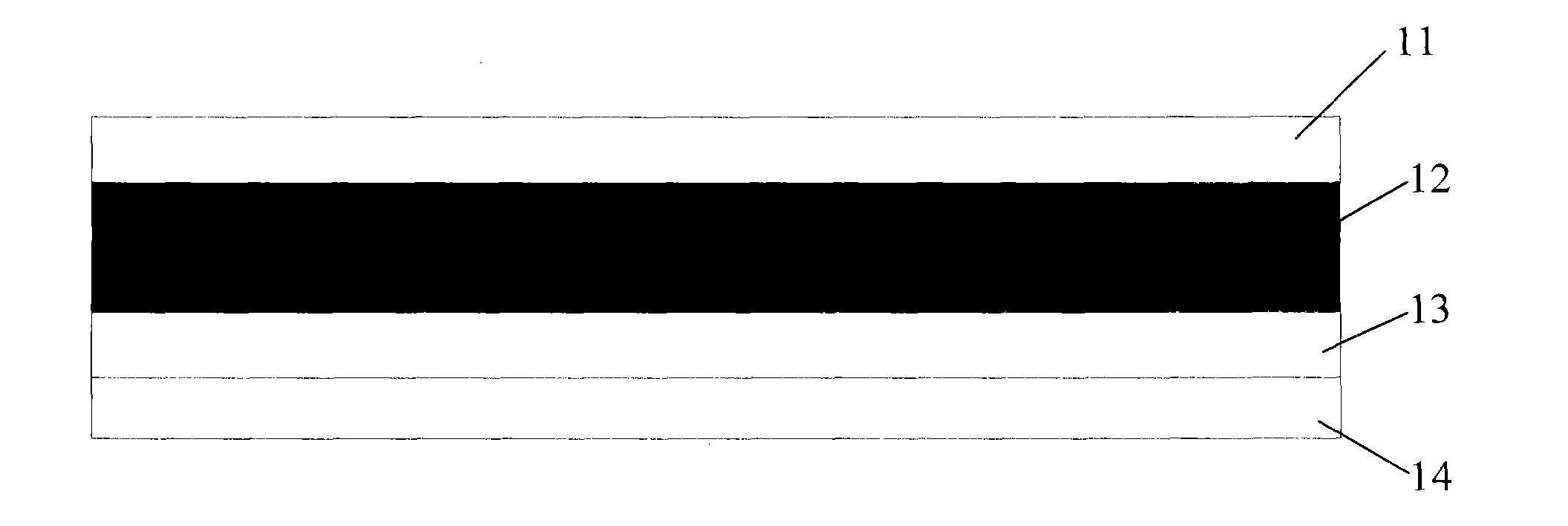
[0036] Embodiment 2 provides a veneer shielding structure, which is basically the same as the veneer shielding structure given in Embodiment 1. The difference is that the structure of the shielding film in the veneer shielding structure is as follows: Figure 4 As shown, it is a laminated structure formed by an insulating layer 21 , a wave absorbing layer 22 , a second insulating layer 23 and an adhesive layer 24 . Wherein, the wave-absorbing layer is made of wave-absorbing material, and the wave-absorbing material can be a material capable of absorbing electromagnetic waves, and its thickness can also reach 0.05-0.2mm. Other parts of the shielding structure of the veneer in this embodiment are basically the same as the shielding structure given in Embodiment 1, and reference may be made to the description of Embodiment 1, which will not be repeated here.
[0037] The shielding film used in the shielding structure of this embodiment also has the same characteristics as the shi...
Embodiment 3
[0039] Embodiment 3 provides a method for realizing a single-board shielding structure, such as Figure 5 As shown, the method includes:
[0040] Step A, setting the shielding frame on the veneer, setting partition ribs in the shielding frame, and separating each radiation source of the veneer through the partition ribs;
[0041]Step B, attaching a covering shielding film on the shielding frame after the ribs are provided, and cooperating the shielding film and the shielding frame to form a closed shielding structure in the shielding frame.
[0042] In step A of the above method, the shielding frame is arranged on the single board by welding and fixing the shielding frame on the single board, so that the shielding frame surrounds the radiation source to be shielded on the single board.
[0043] In step B of the above method, attaching and covering the shielding film on the shielding frame after the ribs are provided specifically includes: pasting and covering the shielding fi...
PUM
 Abstract
Description
Claims
Application Information
 - R&D
- Intellectual Property
- Life Sciences
- Materials
- Tech Scout
- Unparalleled Data Quality
- Higher Quality Content
- 60% Fewer Hallucinations
Browse by: Latest US Patents, China's latest patents, Technical Efficacy Thesaurus, Application Domain, Technology Topic, Popular Technical Reports.
© 2025 PatSnap. All rights reserved.Legal|Privacy policy|Modern Slavery Act Transparency Statement|Sitemap|About US| Contact US: help@patsnap.com


