
Method and system for forming blind gongs on printed circuit board (PCB) and circuit board

A technology for printed circuit boards and printed circuit boards, which is applied in manufacturing tools, printed circuits, printed circuit manufacturing, etc., can solve the problem of affecting the precision of blind gong processing, difficult to control the depth of blind gongs, and easy warping of bakelite boards on auxiliary platforms. It can avoid the problem of low precision and accurately control the depth.

Active Publication Date: 2012-12-26
CHONGQING FOUNDER HI TECH ELECTRONICS +1
View PDF0 Cites 1 Cited by
  • Summary
  • Abstract
  • Description
  • Claims
  • Application Information

AI Technical Summary

Problems solved by technology

The machining accuracy of the blind gong molding machine is high, but there are some problems with the auxiliary platform bakelite board, for example: the thickness of the auxiliary platform bakelite board has a tolerance of ±0.1mm, or the auxiliary platform bakelite board is easy to warp
In this way, it is difficult to control the depth of blind gongs during PCB blind gong processing, which seriously affects the accuracy of blind gong processing.

Method used


Image

  • Method and system for forming blind gongs on printed circuit board (PCB) and circuit board
  • Method and system for forming blind gongs on printed circuit board (PCB) and circuit board
  • Method and system for forming blind gongs on printed circuit board (PCB) and circuit board

Examples


Embodiment Construction

[0023] In the embodiment of the present invention, when the blind gong is processed on the PCB, the PCB to be blind gong is directly fixed on the machine table of the blind gong forming machine, thus avoiding the low processing precision caused by the auxiliary platform bakelite The problem.

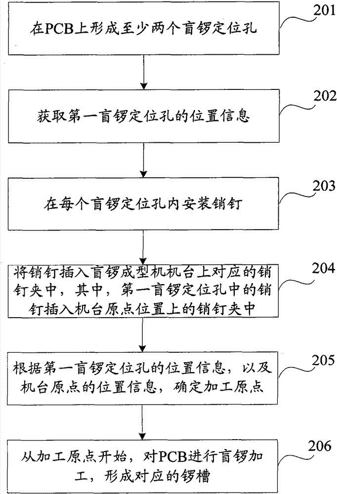
[0024] see figure 2 , in the embodiment of the present invention, the process of PCB molding blind gong processing includes:

[0025] Step 201: Form at least two blind gong positioning holes on the PCB.

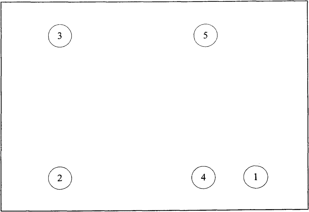
[0026] In order to fix the PCB to the machine table of the blind gong molding machine, generally at least two blind gong positioning holes are required. Two or more blind gong positioning holes can be formed in free positions on the PCB. Of course, in order not to affect the positioning holes required by other processes, preferably, at least two blind gong positioning holes are formed on the set positions of the PCB. Generally, two or more blind gong positioning holes can be formed...


PUM


Abstract

The invention discloses a method and system for forming blind gongs on a printed circuit board (PCB) and a circuit board to improve the precision of machining the blind gongs on the PCB. The method comprises the following steps: forming at least two blind gong locating holes on the PCB and obtaining the location information of the first blind gong locating hole; installing a pin in each blind gong locating hole and inserting each pin into a corresponding pin clip on a bench of a blind gong forming machine, wherein the pin in the first blind gong locating hole is inserted into the pin clip on the location of an origin of the bench; and determining the machining origin according to the location information of the first blind gong locating hole and the origin on the bench and beginning machining the blind gongs on the PCB from the machining origin to form corresponding gong slots.

Description

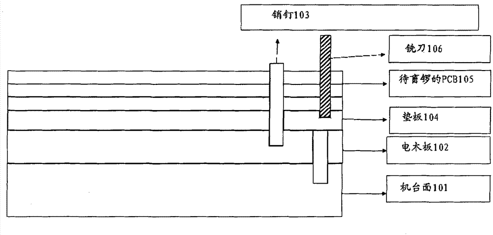
technical field [0001] The invention relates to the technical field of printed circuit board production, in particular to a method, system and circuit board for forming blind gong processing of printed circuit boards. Background technique [0002] At present, the production process of a typical printed circuit board (PCB) is as follows: blanking→inner layer production→pressing→drilling→copper plating→outer layer production→solder resist printing→text printing→surface Processing → shape processing. Because some products need to install part of the components into the PCB board, therefore, in the shape processing process of these PCBs, it is necessary to carry out gong grooves on the PCB board, that is, blind gong processing. [0003] Generally, blind gong processing is carried out on PCB by blind gong forming machine, see figure 1 , fix the auxiliary platform bakelite board 102 on the machine table 101 of the blind gong forming machine, then implant pins 103 on the auxiliar...

Claims


Application Information

Patent Timeline
Patent Type & Authority Patents(China)
IPC IPC(8): H05K3/00H05K1/02B23C3/28
Inventor 蒋明川
Owner CHONGQING FOUNDER HI TECH ELECTRONICS
Learn More